Tungsten Diselenide (WSe2) Few-layer Film
CAS Number 12067-46-8
2D Materials, Low Dimensional Materials, Materials, Transition Metal Chalcogenides (TMCs), Transition Metal Dichalcogenides (TMDs)
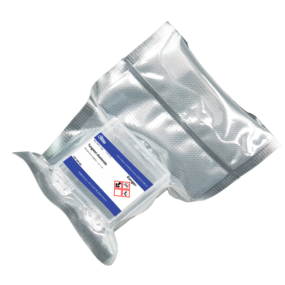
High purity tungsten diselenide few-layer film
For applications in transistors, sensors, photovoltaics, and photodetectors devices
Technical Data | MSDS | Applications | Literature and Reviews | Related Products | Resources and Support
Tungsten diselenide (WSe2) few-layer film, CAS number 12067-46-8, based field-effect transistors (FETs) can display high hole mobilities ranging from 350 cm2/Vs at room temperature to the saturating value of ~500 cm2/Vs below 50 K. Tri-layered WSe2 shows a strong photocurrent response of exceptionally high photo responsivities up to 7 A/W under white light illumination and external quantum efficiencies approaching 40% (under laser illumination at λ = 532 nm).
It also has been demonstrated that the carrier type evolves with increasing WSe2 channel thickness, from p-type (<3 nm) to ambipolar (~4 nm) and n-type (>5 nm). The thickness dependent carrier type is due to the changes in the bandgap of WSe2 as a function of the thickness and their band offsets relative to the metal contacts. WSe2 few-layers also exhibit drastic increase in photoluminescent intensity under the application of uniaxial tensile.
High Purity
≥99.999% Crystal Purity
Worldwide shipping
Quick and reliable shipping
Low Cost
Low Cost Tungsten Diselenide
Applications
Applications in Photovoltaics, Photodetectors, FETs and Biomedical
Technical Data
| CAS Number | 12067-46-8 |
| Chemical Formula | WSe2 |
| Molecular Weight | 341.76 g/mol |
| Bandgap | Indirect bandgap |
| Synonyms | Tungsten selenide, Tungsten(IV) Selenide |
| Classification / Family | Transition metal dichalcogenides (TMDCs), 2D semiconductor materials, Nano-electronics, Nano-photonics, Materials science |
Product Details
| Substrate | Sapphire - Double Side Polished |
| Product Code | M2224F11 |
| Size | 1 cm × 1 cm* |
| Growth Method | CVD synthesis |
| Appearance | Transparent |
| Purity | >99% |
| Transparency | >97% |
| Coverage | >95% |
| Number of Layers | 1 |
| Sheet Resistance | N/A |
| Transfer Method | Directly grown |
*Other sizes available: up to 2 cm × 2 cm or 2 inches in diameter.
High-quality tungsten diselenide (WSe2) few-layer films are available on Sapphire as standard. Different substrates of few-layer WSe2 films, including SiO2/Si, Glass, Silicon and Quartz are also available via custom order.
Please contact us for more information regarding custom products.
MSDS Document
 Tungsten Diselenide Few-Layer Film MSDS Sheet
Applications
- Field-effect transistors (FETs)
- Photodetectors
- Photovoltaics
- Sensors
- Biomedical
Synthesis
Tungsten diselenide (WSe2) few-layer film was directly grown on a double side polish sapphire.
Literature and Reviews
-
High Photoresponsivity and Short Photoresponse Times in Few-Layered WSe2 Transistors, N. Pradhan et al., ACS Appl. Mater. Interfaces, 7 (22), 12080–12088 (2015); DOI: 10.1021/acsami.5b02264.
-
Hall and field-effect mobilities in few layered p-WSe2 field-effect transistors, N. Pradhan et al., Sci. Rep., 5, 8979 (2015); DOI: 10.1038/srep08979.
-
Accurate identification of layer number for few-layer WS2 and WSe2 via spectroscopic study, Y. Li et al., Nanotechnology, 29, 124001 (2018); DOI 10.1088/1361-6528/aaa923.
Related Products
We stock a wide range of 2D materials available to purchase online. Please contact us if you cannot find what you are looking for.