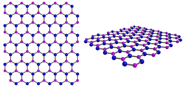
Hexagonal Boron Nitride (h-BN) Structure
Hexagonal boron nitride (h-BN) has a layered structure. In a layer of h-BN, each boron atom is covalently bonded to three nitrogen atoms and vice versa. This creates a "honeycomb" or hexagonal lattice structure similar to that of graphene materials. Due to the similarity in structure, h-BN is often referred to as "white graphene".

Hexagonal Boron Nitride Bonds
The experimental bond length hexagonal boron nitride (h-BN) sheets ranges from 1.4-1.6 Å. A single layer of h-BN is 0.44 nm thick (Cartamil-Bueno et al., 2017).
Boron nitride crystallises in hexagonal form at room temperature and normal pressure. It is the most stable phase of the three crystalline forms (which include cubic and wurtzite). Whilst there are strong bonds within the hexagonal layers the inter-layer interactions are weak van der Waals forces. This makes h-BN easy to exfoliate to access the individual 2D h-BN layers. Similar to exfoliating graphite to 2D graphene.
The in-layer bonds between boron and nitrogen are sp2 hybridized. Boron and nitrogen have different electronegativities (nitrogen = more electronegative). This difference means electrons within the covalent bond are more attracted to the nitrogen atoms. This creates an electron dipole at each B-N bond with partial ionic character. This is referred to as polar covalent bonding. This is very different to graphene where all atoms are carbon.
The bonds in hexagonal boron nitride arrange themselves in a planar triangular geometry. This configuration means in-plane bonds are strong and contributes to the unique properties of h-BN which include:
- Electrical insulation
- Thermal conductivity
- Chemical stability
- Mechanical strength
- Low friction coefficient
- Optical properties
- Neutron shielding
- Biocompatibility
Hexagonal Boron Nitride Band Structure
The band structure of hexagonal boron nitride is dictated by the alternating boron and nitrogen atoms. There are different potential energies for the electrons associated with the atoms. This is due to their different electronegativities (boron - 2.04 vs nitrogen - 3.04). This creates an asymmetry in the electronic band structure.
| Electronegativity | p-orbital energy | Electron Orbital Band | |
|---|---|---|---|
| Nitrogen | Higher | Lower | Valence (More Filled) |
| Boron | Lower | Higher | Conduction (Less Filled) |
The electrons in the p-orbital of nitrogen are lower in energy. This is due to the higher electronegativity of nitrogen. The valence band which is mostly derived from nitrogen p-orbitals is more filled.The electrons in the p-orbital of boron are higher in energy. This is due to the lower electronegativity of boron. The conduction band which is mostly derived from the p-orbitals of boron is less filled. The significant energy different between the conduction and valence band results in hexagonal boron nitride having a large band gap compared to other hexagonal 2D materials like graphene (no band gap).
Hexagonal Boron Nitride Band Gap
An isolated 2D monolayer of hexagonal boron nitride has a direct band gap of ~6 eV. It is classed as a wide-band gap semiconductor. This is because the lowest energy of the conduction band and the highest energy of the valence band occur at the same point in the Brillouin zone. This is typically the K point. The direct nature of the band gap means that electronic transitions can occur without a change in the momentum of the electrons.
The direct wide-band gap of 2D hexagonal boron nitride makes it suitable for high-power and high-frequency applications. As well as for optoelectronics including in deep ultraviolet (DUV) applications as an active layer with highly efficient light–matter coupling.
Bulk hexagonal boron nitride powder is an semiconductor with an indirect-band gap of 5.95 eV. As thickness of h-BN increases above a monolayer the band gap becomes indirect. The lowest energy of the conduction band and the highest energy of the valence band occur at different points in the Brillouin zone. This is a similar crossover to indirect as observed with molybdenum disulfide (MoS2).
Hexagonal Boron Nitride

Learn More
Resources and Support
- Cartamil-Bueno, S. J. et al. (2017). Mechanical characterization and cleaning of CVD single-layer h-BN resonators. npj 2D Materials and Applications volume, 1, doi:10.1038/s41699-017-0020-8
- Elias, C. et al. (2019). Direct band-gap crossover in epitaxial monolayer boron nitride. Nat Commun, 10, doi:10.1038/s41467-019-10610-5
- Cassabois, G. et al. (2016) Hexagonal boron nitride is an indirect bandgap semiconductor Nat. Photon., 10, doi:10.1038/NPHOTON.2015.277
Contributors
Written by
Application Scientist
Diagrams by
Graphic Designer

