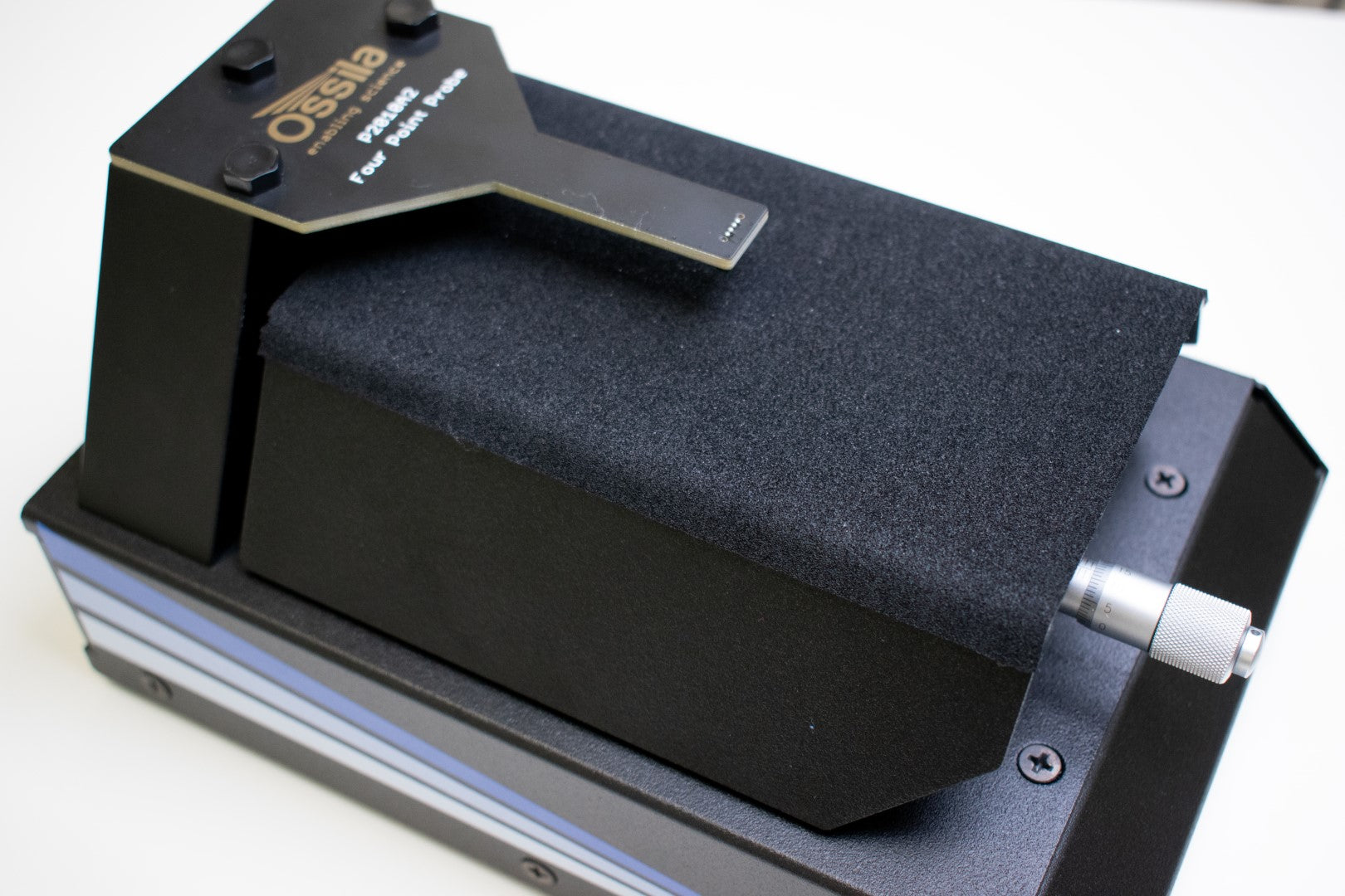
Getting Started with the Ossila Four-Point Probe

What is a Four-Point Probe?
The four-point probe is the most commonly-used piece of equipment for measuring the sheet resistance of a material. Sheet resistance is the resistivity of a material divided by its thickness, and represents the lateral resistance through a thin square of conducting/semiconducting material. This measurement uses four probes arrayed in a line, with equal spacing between each probe. A current is passed between the outer two probes, causing a reduction in voltage between the inner two probes. By measuring this change in voltage, the sheet resistance can then be calculated.
Getting Started
Sheet Resistance Equation
Sheet resistance can be calculated using the following equation:

Here, I is the applied current and ΔV is the decrease in voltage between the inner probes. The result of this equation must further be multiplied by a geometric correction factor based upon the shape, size, and thickness of the sample. This accounts for limitations to the possible current pathways through the sample, which affects the values that are measured.
Sample Thickness
The Four-Point Probe System is specifically designed to enable the measurement of thin films in the nanometre range. For example, we have successfully measured 30 – 40 nm films of PH 1000 PEDOT:PSS (a PEDOT:PSS formulation) and <100 nm silver nanowire films on PET, without creating holes in the thin films.
Applications
Sheet resistance is an important property of materials, which is commonly used in material characterisation and in the development of thin-film devices such as perovskite solar cells or organic LEDs.
Material Characterisation
Resistivity is an inherent characteristic of a material, and an important electrical property. It can be determined by measuring the sheet resistance of a thin film with a known thickness, making the four-point probe measurement a key technique for the electrical characterisation of materials.
Thin-Film Solar Cells and LEDs
Thin-film devices require thin conducting electrodes that transport electrical charge laterally to be extracted, so materials with low sheet resistances are required to reduce potential losses. This becomes even more important when attempting to scale up these devices, as the electrical charges must travel further along the electrodes before they can be extracted.

Materials that are not compatible with the system are those that can form oxide layers, causing no contact between probe and sample. Examples of such materials include semiconductors consisting of pure silicon and those that fall within the III-V category (GaAs, InP, AlAs, etc).
Four-Point Probe
