Hafnium Disulfide (HfS2) Powder and Crystal
CAS Number 18855-94-2
2D Materials, Low Dimensional Materials, Materials, Transition Metal Chalcogenides (TMCs), Transition Metal Dichalcogenides (TMDs)Low price, high purity 2D hafnium disulfide powder and crystals
For the development of next-generation electronics, optoelectronics, and nanotechnology
Technical Data | MSDS | Structure | Literature and Reviews | Related Products | Resources and Support
Hafnium disulfide (HfS2), CAS number 18855-94-2, is layered 2D semiconducting material that is part of the group IV transition metal dichalcogenides (TMDCs). Hafnium disulfide is a semiconductor with an indirect band gap of ~ 2.0 eV. Single layers of HfS2 are predicted to have a direct band gap of ~1.2 eV.
High Purity
High purity 2D hafnium disulfide
Worldwide shipping
Quick and reliable shipping
Low price
Low price Hafnium Disulfide (HfS2)
Powder & Crystals
Available in powder and crystal forms
Hafnium disulfide (HfS2) powder has a layered structure. Each layer is bound by weak van der Waals forces. Ultra-thin films of HfS2 can be chemically-exfoliated from its layered bulk powder form. HfS2 crystallises with octahedral metal coordination in the 1T polytype. 1T-HfS2 is semiconducting in nature. Ultrathin HfS2 shows a higher, faster response and higher stability than most other two-dimensional materials. However, the 1T-HfS2 monolayer system undergoes a semiconductor-to-metal transition while compressive strain is applied.
We supply low price hafnium disulfide in several different forms for a range of applications.

Hafnium Disulfide Powder
Can be used for preparation of hafnium disulfide nanoplates and ultrathin films
Available in quantities of 1g
≥ 99.995% purity
From £350

Hafnium Sulfide Crystals by Size
Can be used to produce single or few-layer hafnium disulfide sheets via mechanical or liquid exfoliation
Small (≥10 mm2) crystal available*
≥99.999% purity
From £520
*Typical representative size, areas/dimensions may vary.
Bulk single hafnium disulfide crystal is most commonly used as sources from which single or few-layer sheets can be obtained via either mechanical or liquid exfoliation. Single hafnium disulfide crystal or films produced from such crystals are suitable for study using atomic force microscopy or transmission electron microscopy.
Few-layer HfS2 nanosheets and nanoparticles can also obtained from hafnium disulfide powder by liquid-exfoliation.
Technical Data
| CAS Number | 18855-94-2 |
| Chemical Formula | HfS2 |
| Molecular Weight | 242.62 g/mol |
| Bandgap | ~2.0 eV (indirect), ~1.2 eV (direct) |
| Preparation | Synthetic - Chemical Vapour Transport (CVT) |
| Structure | Octahedral (1T) |
| Electronic Properties | 2D Semiconductor |
| Melting Point | N/A |
| Colour | Dark brown |
| Synonyms | Hafnium sulfide |
| Classification / Family | Transition metal dichalcogenides (TMDCs), 2D Semiconductor materials, Nano-electronics, Nano-photonics, Photovoltaic, Materials science |
Product Details
| Form | Purity |
|---|---|
| Powder | ≥99.995% |
| Crystal | ≥99.999% |
Pricing Table
| Product Code | Form | Size/Weight* | Price |
|---|---|---|---|
| M2152C1 | Powder | 1 g | £350 |
| M2152A10 | Crystal | Small (≥10 mm2) | £520 ea. |
*typical representative size, areas/dimensions may vary.
Shipping is free for qualifying orders.
MSDS Documents
Structure of Hafnium Disulfide
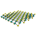
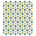
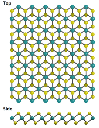
Hafnium disulfide (HfS2) adopts the CdI2 structure (1T structure) with a single-layer plane of hexagonal close-packed Hf atoms sandwiched by two-layer planes of hexagonal close-packed S atoms. The layers are stacked together by weak van der Waals (vdW) interactions, and can be exfoliated into thin 2D layers.

Properties of Hafnium Disulfide
After exfoliation of hafnium disulfide crystal or powder, hafnium disulfide typically has the following properties:
- Octahedral (1T, space group: P3m1)
- Group IV transition metal dichalcogenides (TMDCs)
- Hafnium disulfide is a semiconductor with an indirect band gap of ~ 2.0 eV. Single layers of HfS2 are predicted to have a direct band gap of ~1.2 eV
- 1T-HfS2 is semiconducting in nature
- 1T-HfS2 monolayer system undergoes a semiconductor-to-metal transition while compressive strain is applied
Applications of Hafnium Disulfide
Hafnium disulfide (HfS2) single crystals can be used to prepare monolayer and few-layer HfS2 by mechanical or liquid exfoliation.
Hafnium disulfide powder is suitable for liquid chemical exfoliation to prepare HfS2 nanosheets and nanoparticles down to few-layer films.
Hafnium disulfide based field-effect transistors (FETs) can have sheet current densities of up to 650 μA μm−1 (about 85 times higher than that of MoS2), making HfS2 an attractive candidate for applications in logic and optoelectronic devices. Exfoliated few-layer HfS2 has also been built into ultra-sensitive photo-transistors and high-performance FETs.
Exfoliated ultra-thin films of HfS2 have an indirect bandgap of ~ 1.2 eV, with high stability against surface degradation. FET based on HfS2 nanosheets gave a high current on/off ratio over 10,000 at room temperature. Photodetectors based on HfS2 nanosheets provide high photosensitivity to 405 nm lasers, with a large on/off ratio of ca. 103 and ultrafast response performance (with rise and fall times of 24 ms).
2D-HfS2 can also be used as an efficient photocatalyst for water splitting, with a strong absorption mainly in the visible and ultraviolet regions.
Literature and Reviews
- Selective Direct Growth of Atomic Layered HfS2 on Hexagonal Boron Nitride for High Performance Photodetectors, D. Wang et al., Chem. Mater.,30, 3819−3826 (2018); DOI: 10.1021/acs.chemmater.8b01091.
- Impact of Metal Contacts on the Performance of Multilayer HfS2 Field-Effect Transistors, X. Nie et al., ACS Appl. Mater. Interfaces, 9, 26996−27003 (2017); DOI: 10.1021/acsami.7b06160.
- 2D-HfS2 as an efficient photocatalyst for water splitting, D. Singh et al., Catal. Sci. Technol., 6, 6605–6614 (2016); DOI: 10.1039/c6cy01172a.
Related Products
We stock a wide range of 2D materials available to purchase online. Please contact us if you cannot find what you are looking for.

 Hafnium disulfide powder

