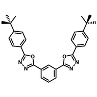
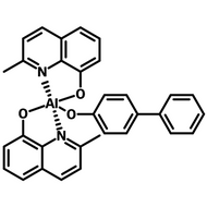
Charge Transport Layer Materials
Charge transport layer (CTL) materials play a crucial role in electronic devices, enabling the separation and transport of charge carriers—electrons and holes. Their functionality and effectiveness are defined by their structure and electronic properties, which offer the following key features:
- Efficiently separate and transport charge carriers (electrons or holes).
- Performance depends on energy level alignment and material structure.
- Organic CTLs are often aromatic and conjugated, enhancing their conductivity.
Electron transport layer (ETL) materials are used within electronic devices to promote electron movement with hole blocking capability. The popular ETL material bathocuproine (BCP) has a wide bandgap, offering excellent exciton blocking properties. Selecting an electron transport layer material with the appropriate LUMO energy level, which aligns well with the cathode, is crucial to maximise charge transport efficiency.
Hole transport layer (HTL) materials, on the other hand, are optimized for transporting holes while blocking electrons from reaching the anode. The common HTL material spiro-OMeTAD exhibits a high-lying LUMO energy level and excellent hole mobility. Both are key features of effective HTL materials.
Materials may also inject charge carriers into the electronic device. These layers are particularly important in organic light-emitting diodes (OLEDs), where the electron affinity of the materials is typically lower than in other organic devices. Including either or both charge injecting layers can often result in decreased device operating voltages.
- Electron injection layers (EIL) aim to significantly reduce the work function around the cathode.
- Hole injection layers (HIL) aim to reduce the energy barrier between the anode and other layers within the device.
These molecules are suitable for OLED applications and in the fabrication of other organic electronic devices such as OFETs, OPVs and perovskite solar cells (PSCs). Maximize your device efficency by fabricating and testing new devices in a glove box environment.
Jump to: Browse Materials by Role | Browse all Charge Transport Layer Materials | Resources and Support
Browse Charge Transport Layer Materials by Role
Browse Charge Transport Layer Materials
Related categories: Semiconducting molecules, Dopant materials, Host materials, TADF materials, OLED materials
Filter by transport layer:
Filter by purification technique:
Resources and Support
Two commonly used materials for hole selective layer (HSL) or hole transport layer (HTL) are PEDOT:PSS (poly(3,4-ethylenedioxythiophene) polystyrene sulfonate) and self-assembled monolayers (SAMs). Each offers distinct advantages and limitations that impact their effectiveness in solar cells.
Read more...PTAA and Spiro-OMeTAD are both used as hole transport layers in high efficiency perovskite solar cells (PSCs). Regular architecture devices using PTAA and Spiro-OMeTAD layers have demonstrated power conversion efficiencies (PCEs) of over 22% and 25% respectively.
Read more...


