Methylammonium Iodide (MAI)
CAS Number 14965-49-2
Materials, Perovskite Materials, Perovskite Precursor Materials,Methylammonium iodide, precursor for the synthesis of perovskites
High quality, low price, and available online for fast and secure dispatch
Overview | Specifications | MSDS | Pricing and Options | Resources and Support
Methylammonium iodide (MAI), CAS number 14965-49-2, also referred to as methylamine hydroiodide, is a precursor for the synthesis of organic-inorganic hybrid perovskites for use in FETs, LEDs and PVs.
Methylammonium Iodide (MAI) from Ossila was used in the high-impact paper (IF 30.85), Strontium Insertion in Methylammonium Lead Iodide: Long Charge Carrier Lifetime and High Fill-Factor Solar Cells, D. Pérez-del-Rey et al., Adv. Mater., 28, 9839-9845 (2016); DOI: 10.1002/adma.201603016.
Specifications
| Chemical Formula | CH6IN |
|---|---|
| Synonyms | Methylamine hydroiodide |
| CAS No. | 14965-49-2 |
| Chemical Name | Methylammonium iodide |
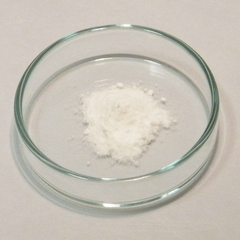
| Physical Aappearance | White, crystalline solid |
| Purity |
M272: 99.9% (ICP-OES) M271: >99.9% (further purified by double recrystallisation from 99.9% grade in ethanol) |
| Molecular Weight | 158.97 g/mol |
| Recommended Solvents (for perovskite synthesis) | DMF, DMSO |
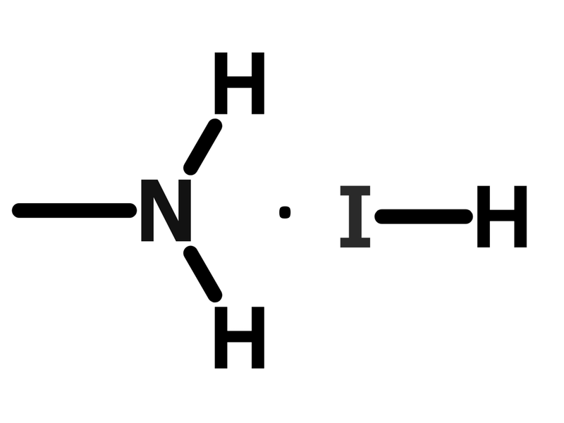
Chemical Structure

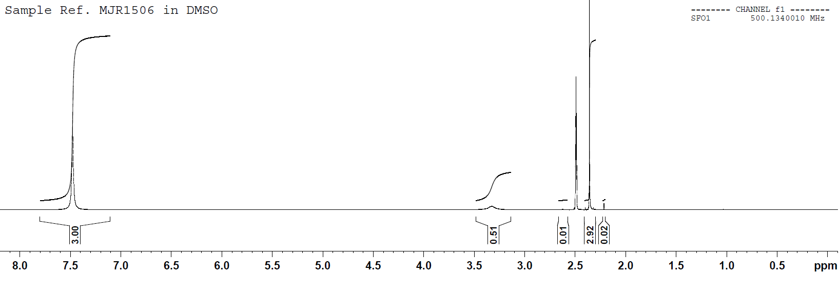
NMR spectrum

MSDS Documentation
 Methylammonium Iodide MSDS sheet
Applications
Due to the high purity of the methylammonium iodide (>99.9% recrystallized), it should be noted that its solubility is reduced within dimethyl formamide and dimethyl sulfoxide. This reduced solubility is due to the removal of trace amounts of residual hydroiodic acid (HI) used during the synthesis and purification of the material. This can potentially have an impact upon the performance of solar cells leading to a reduction in maximum power conversion efficiency achievable. Adding fixed concentrations of hydroiodic acid to perovskite solutions can allow for the improvement of device metrics[1-3]. Using high-purity precursor materials allows for accurate addition of amounts of hydroiodic acid giving higher reproducibility to experiments. It is recommended that between 1% and 10% hydroiodic acid is used with high-purity methylammonium iodide to achieve optimal device performance. The amount required depends on the precursors used, solution concentration, solvent used, and processing environment. Therefore, this will need to be adjusted for each individual laboratory and process.
For simpler ink fabrication, it is recommended that the lower-purity methylammonium iodide (99.9% non-recrystallized) is used.
- Hysteresis-less inverted CH3NH3PbI3 planar perovskite hybrid solar cells with 18.1% power conversion efficiency, J. H. Heo et al., Energ. Environ. Sci., 8, 602-1608 (2015); DOI: 10.1039/C5EE00120J.
- A [2,2]paracyclophane triarylamine-based hole-transporting material for high performance perovskite solar cells, S Park et al., J. Mater. Chem. A., 3, 24215-24220 (2015); DOI: 10.1039/C5TA08417B.
- Enhanced optopelectronic quality of perovskite thin films with hydrophosphorous acid for planar heterojunction solar cells, W. Zhang et al., Nat. Commun., 6, 10030 (2015); doi:10.1038/ncomms10030.

Usage details
Reference devices - perovskite PVs
Reference devices were made to assess the performance of perovskite (MAI:PbCl2) based devices with the below structure. These were fabricated in air prior to spincasting the fullerene layer in a N2 glove box Substrates were then transferred to a vacuum chamber where a composite metal cathode was thermally evaporated. Finally, substrates were encapsulated inside the glove box before measurements were taken under ambient conditions.
Glass / ITO (100 nm) / PEDOT:PSS (30 nm) / MAI:PbCl2 / PC70BM / Ca (5 nm) / Al (100 nm)
For generic details please see the fabrication guide and video. For specific details please see the below condensed fabrication report which details the optical modelling and optimisation of the multilayer stack.
The perovskite solution (MAI:PbCl2 at a molar ratio of 3:1) was made in dimethylformamide (DMF) at a concentration of 664 mg/ml. It was found to be critical that both materials were mixed dry prior to adding the solvent in order to achieve such high concentration.
For maximum efficiency, the active layer thickness was achieved from spin casting the heated solution (70°C) onto a hot PEDOT:PSS substrate (90°C) at a spin speed of 5000 rpm for 30s. The films were then placed back onto the hotplate (90°C) for 2 hrs. The data below shows the maximum performance achieved from non-optimised conditions.
Overall, the average efficiency after 5 mins light soaking was 8.89% (9.57% maximum) from MAI:PbCl2 based devices. Hysteresis was observed to be quite significant, with sweeps running from positive to negative bias presenting the best efficiencies (hereby referred to as reverse sweeps).


Fabrication
Substrates and cleaning
- Pixelated Cathode substrates (S171) or Photovoltaic (8 Pixel) Substrates
- 5 minutes sonication in hot 1% Hellmanex III
- 1x boiling DI dump rinse, 1x cold dump rinse
- 5 minutes sonication in warm IPA
- 2x DI cold dump rinse
- Stored in DI for 1hr
- 5 minutes sonication in hot 10% NaOH solution
- 2x DI dump rinse
- N2 blow dry
PEDOT:PSS
- PEDOT:PSS (AI 4083 PEDOT:PSS) filtered through a 0.45 µm PES filter (C2009S1)
- Spin on heated substrates at 6000 rpm for 30s
- Bake at 130°C after spin cast
- Note that the cathode strip was not wiped clean, this is to allow a consistent perovskite layer on top
- Substrates held at a temperature of 90°C for spin casting
Active layer solution
- Old stock solution (2 weeks old) of MAI:PbCl2 (3:1 molar ratio) made at a concentration 664 mg/ml in DMF
- Heated for approx. 3 hrs at 70°C
- Old stock solution of PC70BM, 50 mg/ml in CB
- Heated for approx. 4 hrs at 70°C with stir bar
Active layers
- Devices spun onto hot substrate at 5000 rpm using 25 µl dynamic dispense for 30s
- Placed immediately onto hotplate at 90°C for 2 hrs
- Cathode wipe with dry cotton bud once all substrates were spun
- Films started with a bright yellow colour
- Changed to a dark grey colour during thermal annealing process
- Transferred to a N2 glove box
- PCBM layer was spun at 1000 rpm for 30s, 20 µl dynamic dispense
- CB cathode wipe
Evaporation
Left in vacuum chamber overnight and evaporated with the below parameters.
- 5 nm Ca at 0.2 Å/s
- 100 nm Al at 1.5 Å/s
- Deposition pressure 1e-6 mbar
Encapsulation
- As standard using Ossila EE1, 30 mins UV in MEGA LV101
Measurements
- JV sweeps taken with source-meter
- Illumination by solar simulator with 100 mW/cm2 AM1.5 output
- NREL certified silicon reference cell used to calibrate
- Lamp current: 7.8 A
- Solar output at start of testing: 1.00 suns at 23°C
- Solar output at end of testing: 1.00 suns at 25°C
- Air cooled substrates
- Room temperature at start of testing : 25°C
- Room temperature at end of testing: 25°C
- Calibrated aperture mask size: 0.256 mm2
We are continuously studying MAI and perovskites and expect to provide you with further information and optimised fabrication guides as we do so. Check back regularly or subscribe to our email newsletter for updates. In the meantime, please contact us if you have any further questions.
Pricing
| Grade | Order Code | Quantity | Price |
|---|---|---|---|
| 99.9% purity | M272 | 10 g | £130 |
| 99.9% purity | M272 | 25 g | £260 |
| 99.9% purity | M272 | 100 g | £760 |
| 99.9% purity | M272 | 500 g | £2300 |
| >99.9% recrystallised | M271 | 5 g | £150 |
| >99.9% recrystallised | M271 | 10 g | £230 |
| >99.9% recrystallised | M271 | 25 g | £460 |
Note: Looking for a bulk order (100 g or above)? Please contact us for a quote.
