Perovskite Materials
Perovskite materials are defined by their unique ABX3 crystal structure, where "A" and "B" are cations and "X" is an anion.
The composition and stoichiometry of perovskite crystals can be altered to fit many different uses. They’re potential applications are only beginning to be explored, but some of the most popular uses of perovskites are in solar cell, LEDs, sensors and photodetectors.
Perovskites often utilize multiple A, B and X components in one crystal to achieve ideal material properties (e.g. for bandgap tuning, stability improvements). This stoichiometry is very important and impact device performance significantly. For most perovskite solar cell, precursor salts are mixed into a solution, which can be deposited through various thin film coating methods. This is known as a perovskite precursor solution or perovskite ink.
Jump to: Perovskite Material Collections | Browse all Perovskite Materials | Resources and Support
Perovskite Material Collections
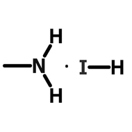
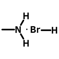
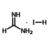
Perovskite Precursor Materials
Browse our range of oganic halide materials for creating perovskite precursors.
Perovskite Interface Materials
Optimize your devices by selecting the right perovskite interface materials for your device.
Browse Perovskite Materials
Related categories: electron / hole transport layers, nanodots and quantum dots, OPV polymers
Filter by popularity:
Filter by collection:
Filter by device role:
Filter by application:
Page 1 of 3
Resources and Support
A perovskite solar cell is a thin film photovoltaic device. In these devices, perovskites absorb sunlight and convert it into electrical energy. Certain perovskites have fundamental properties which make them excellent at this. In some ways, perovskites are even better than the materials used in current solar cells.
Read more...PTAA and Spiro-OMeTAD are both used as hole transport layers in high efficiency perovskite solar cells (PSCs). Regular architecture devices using PTAA and Spiro-OMeTAD layers have demonstrated power conversion efficiencies (PCEs) of over 22% and 25% respectively.
Read more...The rapid improvement of perovskite solar cells has made them the rising star of the photovoltaics world and of huge interest to the academic community.
Read more... History and Evolution of Perovskites
The discovery of perovskite crystals in the Ural Mountains in the 19th century was followed by the discovery of metal halide perovskites some 50 years later.
Read more...Introduction to..
Methylammonium lead iodide (MAPbI3) was one of the first perovskite materials used in perovskite solar cells. These crystal structures combine the organic A cation methylammonium (MA+, CH3NH3+) and divalent lead (Pb+) with three iodide anions (I-).
Read more...Formamidinum lead iodide (FAPbI3) is a material used for perovskite solar cells. FAPbI3 was introduced in 2014 as an alternative to MAPbI3 (Eperon 2014).
Read more...Fabrication and Processing
 The Ultimate Guide to Making Perovskite Solar Cells
Over the past 10 years, perovskite solar cells (PSCs) have achieved record efficiencies of 25.5% single junction solar cells (as of 20211) and these efficiencies are rising impressively.
Read more... Perovskite Fabrication
This guide describes our recommended fabrication routine for perovskite solar cells using Ossila I101 Perovskite Precursor Ink which is designed to be used with a bottom ITO/PEDOT:PSS anode and a top PC70BM/Ca/Al cathode.
Read more...This article aims to introduce some methods that have been adapted to improve perovskite solar cell stability.
Read more...Perovskite solar cells show impressive efficiencies and offer “a different kind of solar cell” that could be cheap to manufacture and could be semi-transparent, lightweight, and flexible.
Read more...More Resources
 Perovskite FAQ
Our technical support team receive enquiries about perovskite solar cell or photovoltaic fabrication on a regular basis. For your convenience, we've collated some of the most common questions here which you may find helpful when using I101 or I201 perovskite precursor inks.
Read more... How humidity affects air processed perovskite films
This video details the effects humidity has on air-processed perovskite films.
Read more...Incorporating self-assembled monolayers (SAMs) within perovskite solar cells has improved device efficiency. SAMs exist as ultrathin layers that can be engineered to improve various aspects of the solar cell including charge transport and stability. SAMs have benefits including:
Read more... Perovskite LEDs
Perovskite LEDs (light emitting diodes), often abbreviated to PeLEDs, use a perovskite material layer to emit light. PeLEDs have many benefits over the common OLED (organic light emitting diodes) and QLED (quantum dot light emitting diodes) alternatives.
Read more...


