Scientific Resources

As part of our mission to help researchers to jump-start their projects and to help our customers get started with our products, we’ve put together a number of written guides, application notes, system overviews, videos, literature reviews and articles. These resources cover the underpinning theory behind our products and their intended applications. In addition, they include a wealth of practical user advice which we have learned from decades of research experience. Learn about how to use and maintain your glove box, or the theory behind inert atmosphere processing and our glove box design principles.
Browse by resource type or product to find what you are looking for or alternatively, navigate to a field-specific page to browse the resources relating to your particular area of interest.
If you need further help with one of our products or advice on their applications, please feel free to contact us to be put in touch with a member of our technical support team. Alternatively, if you do not require a response but would like to make a suggestion, we welcome all comments via our feedback form.
Filter by type:
Filter by field:
Filter by product:
 Battery Materials: The Key to High-Performance Energy Storage
Battery materials are the components that make up a battery, each serving a specific role in storing and harnessing electrical energy. The most well-known components are the electrodes (cathode and anode). Whether it’s a lithium-ion, sodium-ion, nickel, solid-state or other battery technology, the key components of a battery remain mainly unchanged.
Read more... Anode Materials
The anode is the electrode where oxidation (loss of electrons) occurs, meaning it releases electrons during battery discharge. Anode materials are essential for facilitating this process and play a central role in determining a battery’s overall performance, capacity, stability, and safety.
Read more...Cathode materials in lithium-ion batteries (LIBs) are engineered for both exceptional electrical conductivity and long-term stability. The main component of the LIB system is the cathode active material, which serves as the primary source of lithium ions and drives the charge and discharge cycles.
Read more...Binary fission and mitosis are two cell division methods used by living organisms. They are essential for growth, repair and reproduction. Both of the processes have the same goal: formation of new cells. However, they differ in their mechanism, occurrence and complexity. Binary fission enables rapid asexual reproduction in prokaryotes. Mitosis, on the other hand, ensures controlled growth and development in eukaryotes.
Read more... How To Set Up a Microbiology Laboratory
Microbiological laboratories have undergone modernization in the last decade. Through automation and advanced technology, the field has been transformed. Designing and setting up a microbiology laboratory requires careful planning, proper equipment, and adherence to safety standards. Well-structured microbiology laboratory can enhance research capabilities, improve efficiency and have an impact on scientific advancements.
Read more...Serial dilution is a laboratory technique used to systematically reduce the concentration of a solution. This allows accurate measurement and experimental procedures. It is a common technique widely applied in microbiology, chemistry and biochemistry for a variety of applications, including quantification of bacterial cultures, preparing standard solutions, and performing assays.
Read more...Micropipettes are an integral part of any biological or chemical laboratory as precise and accurate handling of liquids is necessary. Micropipettes allow scientists to transfer liquid in small volumes, usually in microliter (µL). The broad application of micropipettes across fields highlights their importance in the modern laboratory.
Read more...Streak plate method is an aseptic technique widely used in microbiological laboratories. It allows researchers to isolate pure cultures and obtain well-isolated colonies of bacteria. The term "streak" refers to a "long, thin line". As such, the method refers to spreading a sample on solid media in the form of such a line. While this method is mainly used to study bacteria, it can be used to isolate yeasts.
Spread plate method is used in microbiological laboratories to isolate and count viable microorganisms within a liquid sample. The method, preferred for its simplicity and cost-effectiveness, provides evenly distributed colonies on solid culture media. It is especially useful for the study of aerobic and facultative aerobic microorganisms.
The pour plate method is a technique used in microbiology to isolate and count viable organisms in liquid samples. Developed in the laboratory of Robert Koch, the technique is especially suitable for facultative, microaerophilic, and anaerobic microorganisms. It is widely used due to it's simplicity, cost-effectiveness and the requirement of minimal resources.
Read more...Mechanism of antimicrobial resistance is a naturally occurring process, which makes common infections harder to treat. Microbes constantly evolve and evade anything that exerts selective pressure on them, including antimicrobials.
Read more...Bacteria, viruses, and fungi are specific microorganisms that interact in different ways with the environment and living organisms. While bacteria can be beneficial or harmful, viruses rely on host cells for reproduction, often causing diseases. Fungi play an important role in decomposition but can also pose health risks. Understanding the differences helps in developing appropriate treatments and preventive measures against infection.
Read more...Microbiological culture serves as a fundamental research tool in molecular biology to study microbial organisms. The method allows the microbes to multiply on a culture media under controlled laboratory conditions. Microbiological cultures are employed in a variety of applications, such as cloning, diagnostics, and environmental monitoring.
Read more...Colony morphology describes the characteristics of cultures. It refers to characteristics visible to the naked eye of both bacterial and fungal colonies growing on an agar plate. It helps researchers to choose the appropriate confirmatory tests. While the methods might look simple, careful observation and examination of colony characteristics are essential in microbiology.
Read more...Ames test is a biological assay widely used for the identification and evaluation of mutagenic potential in chemical compounds. Using bacteria, this test examines whether a specific chemical has the potential to cause mutations in DNA of the organism being tested.
Read more... Cyclic Voltammetry Basic Principles, Theory and Setup
Cyclic voltammetry is an electrochemical technique for measuring the current response of a redox active solution to a linearly cycled potential sweep between two or more set values.
Read more...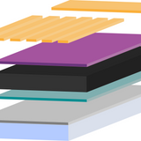 Perovskite Solar Cell Structure and Layers
Over the past 10 years, perovskite solar cells (PSCs) have achieved record efficiencies of 25.5% single junction solar cells (as of 20211) and these efficiencies are rising impressively.
Read more...Perovskite solar cells have significant stability challenges that must be addressed before they can be considered suitable for large-scale manufacturing.
Read more...Cyclic voltammetry is a versatile electrochemical method with a range of different applications. In cyclic voltammetry, each successful forwards and backwards potential sweep produces a 'duck-shaped' plot known as a cyclic voltammogram.
Read more... Dynamic Light Scattering Instrument
Dynamic light scattering (DLS) is a non-invasive measurement technique used to measure the size of colloids or suspended particles in solution.
Read more... Micromanipulator Drift and Other Common Errors
The performance of a micromanipulator can suffer from various mechanical issues, including drift, backlash, side play, and sticking.
Read more... Colony Counting: Method and Tips
Manual colony counting can be tedious and choosing the right colony counter overwhelming. This means it is important for you to understand the benefits and limitations of both automatic and manual colony counters.
Read more... Laminar Flow Hoods: Microbiology, Molecular Biology and Pharmaceuticals
To maintain a clean and germ-free environment in a laboratory, it is a good idea to use a laminar flow hood. These systems are useful for various lab procedures involving safe, non-harmful substances.
Read more...Polymerase chain reaction (PCR), sometimes referred to as ‘molecular photocopying’, is a cost-effective method widely used to make copies of DNA in vitro (in a test tube, not a living organism).
Read more... What are Aseptic Techniques?
Aseptic techniques are essential practices in microbiology and biotechnology. They prevent contamination of samples, equipment, and environments by unwanted microorganisms.
Read more... Agar Plates
Agar plates are important tools in microbiology used by researchers and scientists to study microorganisms. These plates consist of a petri dish with growth medium made of agar.
Read more... What are Sterile Techniques?
The primary goal of sterilization is to get rid of all microorganisms from surfaces and materials. This helps with reducing the risk of contamination and ensuring accurate results.
Read more... Aseptic vs Sterile Techniques
Aseptic techniques focus on preventing contamination. Sterile techniques ensure the complete elimination of microorganisms. Understanding the difference between these two techniques is important when determining the suitable method.
Read more...A perovskite solar cell is a thin film photovoltaic device. In these devices, perovskites absorb sunlight and convert it into electrical energy. Certain perovskites have fundamental properties which make them excellent at this. In some ways, perovskites are even better than the materials used in current solar cells.
Read more... What are Metal Organic Frameworks?
Metal-Organic Frameworks (MOFs) are a class of 3D materials that are made up of metals connected by organic linker compounds. Think of metals and organic compounds as building blocks that form structures. These structures come in a variety of shapes and sizes, ranging from 1D to 3D.
Learn more...Metal-organic frameworks (MOFs) are made by connecting metal centers with organic linkers through coordination bonds. The process of creating MOFs plays a crucial role in crystal structure formation. This determines their properties and how well they perform in various applications.
Learn more...Organic semiconductors are materials, ranging from small molecules to polymers, that can transport charge. Unlike in conductors, where electrons move freely across the material, organic semiconductors rely on a structure primarily composed of carbon and hydrogen atoms.
Read more...Semiconductors are amongst the smallest and most detailed technologies that exist. One thumb-sized chip can contain billions of transistors – the miniature units used for conducting and switching electrical current.
Read more... What is a Polaron?
A polaron refers to the local distortion of a molecular structure or lattice caused by a charge carrier moving through a semiconductor. It represents the combination of both the electron or hole and the displacement of atoms from their equilibrium position within the molecule or lattice.
Read more... What is a Photodetector?
A photodetector is a device that can detect light, or more specifically photons. They are classed as optoelectronic devices like photovoltaic devices. This is because they produce an electronic signal which is proportional to the incident optical input.
Read more...Organic electrochemical transistors (OECTs) regulate charge flow through an organic semiconductor channel via ion injection from an electrolyte. The most common organic semiconductor used is PEDOT:PSS.
Read more... Understanding HOMO and LUMO
HOMO (Highest Occupied Molecular Orbital) and LUMO (Lowest Unoccupied Molecular Orbital) are fundamental concepts in molecular orbital theory. HOMO and LUMO are known as the "frontier molecular orbitals" because they are the highest occupied and lowest unoccupied molecular orbitals, respectively.
Read more...Microfluidics is a ground-breaking field of research focused on the development of fluid-processing technology at the microscale.
Read more...The Internet of Things (IoT), also known as the Internet of Everything (IoE), essentially extends the power of the internet beyond computing devices to other devices, processes and environments.
Read more...Semiconductors are essential features of our daily lives. They enable the receival, processing, and storage of data in modern electronics, including computers and smart phones, to bank cash machines and trains. Within emerging technologies, such as artificial intelligence, the Internet of Things, and quantum computing, semiconductors play a significant role.
Read more...Semiconductors are a material with properties that fall between a good conductor (like metals) and a good insulator (like rubber). Depending on the conditions, semiconductors can be conductive or insulating. This ability to control the flow of electrical current in modern electrical devices, such as microchips and photovoltaics.
Read more...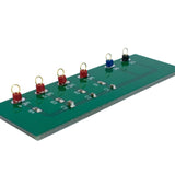 Troubleshooting Cyclic Voltammetry and Voltammograms
Cyclic voltammetry is a powerful and versatile electrochemical technique. With modern potentiostats and software packages, the method is relatively straight-forward to perform. Despite this apparent simplicity, there are still a number of things that can go wrong, particularly when setting up the electrochemical cell.
Read more... How to Perform Cyclic Voltammetry on a Polymer using a Potentiostat
Learn how to perform cyclic voltammetry on a polymer with the Ossila Potentiostat.
Read more... Potentiostat Circuit Diagram
A potentiostat circuit diagram includes both the internal electrical components of the potentiostat, such as amplifiers, feedback loops, and voltage control circuitry, and the external components that make up the electrochemical measurement system (electrochemical cell and electrodes).
Read more... Connecting the Micromanipulator to the Source Measure Unit
This guide gives an overview of how to use the Ossila Micromanipulators with the Source Measure Unit, as well as some general tips and tricks for getting the most out of sensitive electrical probing measurements.
Read more...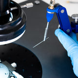 How to Position the Ossila Micromanipulator Probe
Learn how to accurately adjust your micromanipulator probe.
Read more... Video: How to Use the Ossila Electrode Cleaning Polishing Kit
This video will show you what you will find inside the electrode polishing kit and how to prepare the kit for cleaning an electrode.
Read more... How to Choose a Laboratory Glove Box
When buying a glove box, it's important that you choose the most suitable system for your specific lab and experiments. The first question that you should be asking yourself when looking for a glove box is what do I need?
Read more... Video: Overview of the Ossila Glove Box
The Ossila Glove Box is specifically designed to provide a controlled environment for conducting experiments.
Read more...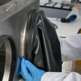 Glove Box Installation
The Ossila Glove Box is designed to be easy to install and maintain, and is suitable for most laboratories. Its small footprint and quick set up also means that it is relatively portable and can be conveniently transferred between labs as required.
Read more... Air Free Techniques
Air free techniques are essential for the handling and storage of materials that are unstable when exposed to air. Compounds are defined as unstable if they react with an element in air, often moisture or oxygen.
Read more...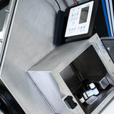 Air Sensitive Compounds
There are many reasons that a compound would be sensitive to air. The magnitude of an air-sensitive material's reaction to oxygen or moisture can vary dependent on the material properties.
Read more... Glove Box Pressure: Positive or Negative?
Glove boxes are essential tools for creating controlled atmospheres where you can handle hazardous or air sensitive materials. They can be maintained at positive pressure or negative pressure.
Read more... Glove Box Standard Operating Procedure
Working safely within an inert laboratory glove box requires care and co-operation from everyone who uses it. For this reason, we recommend outlining a standard operating procedure for your laboratory.
Read more... Inert Gases
Inert gases are gases which are chemically inactive, so will not undergo chemical reactions with many materials. Inert gases are used for many purposes in a wide range of industries - for example in welding, chemical processing, and as filler gases in light sources.
Read more... Argon vs Nitrogen for Glove Box
Argon and nitrogen are both unreactive gases which can be used to create an inert environment within a glove box. Both gases will efficiently displace air within a confined space, are easy to store and will not react with most materials. Therefore, both N2 and Ar can create a glove box environment with very low moisture and oxygen levels.
Read more... Glove Box Maintenance And Troubleshooting
The Ossila Glove Box uses automatic purging and programmable leak tests making it easy to maintain an inert environment. However, there are a number of steps that you as the glove box user can take to ensure that the inert atmosphere remains intact.
Read more...Scientific glove boxes create a sealed environment for work that involves hazardous materials or samples that react with air. The main chamber of such a glove box is generally filled with an inert gas, usually Nitrogen.
Read more... Glove Box Leaks
The most common cause of glove box leaks is human error, either as a result of not following operating procedures correctly or from accidental damage. In terms of physical damage, the most likely puncture points will be the glove box gloves or the seals around the antechamber doors.
Read more... How to Replace Glove Box Gloves
Glove box gloves must be flexible and relatively thin. This allows for movement within the main chamber. The gloves will be the most vulnerable exposure point to air and moisture in your glove box as small holes can easily occur.
Read more... How to Write a COSHH Form
The COSHH (Control of Substances Hazardous to Health) form is a health and safety document that is written for individual substances.
Read more...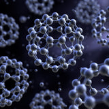 A Simple Introduction to Fullerene: Structure, Properties and Applications
Fullerenes are a special type, or allotrope, of carbon. They are famous for their hollow, cage-like structures typically made entirely of carbon atoms. These carbon atoms are arranged in patterns of hexagons and pentagons, similar to the pattern on a football or a geodesic dome.
Read more... What is Carbon 60 (C60)? Benefits and Properties
Academic research has examined the Nobel Prize-winning molecule carbon 60 (C60) for various applications, including electronics and catalysis. More recently, its potential use in cosmetics and medicine has gained attention. Tests have been conducted globally to evaluate the effects of carbon 60 on human white blood cell cultures and animals.
Read more... What is Laminar Flow?
Laminar flow is a concept in fluid dynamics which describes the smooth and orderly movement of a fluid (liquid or gas). In laminar flow, fluid particles move in predictable, parallel layers with minimal mixing between layers.
Read more... Vertical vs Horizontal Laminar Flow Hood
Laminar flow hoods (LFH) are essential tools used in scientific and industrial settings to create a controlled, clean environment for various applications.
Read more... Laminar Flow Hood vs Fume Hood
In lab environments, both laminar flow hoods and fume hoods operate to provide workspaces with enhanced ventilation and filtration mechanisms.
Read more... Biological Safety Cabinet vs Laminar Flow Hood
When working in laboratories, ensuring a safe and clean environment is paramount. Biological Safety Cabinets and Laminar Flow Hoods are two units that can be used to achieve these standards.
Read more... Laminar Flow Hood vs Glove Box
Laminar flow hoods and glove boxes both provide controlled environments to be used in laboratory settings, but they have distinct differences in terms of their features and functions within the laboratory.
Read more... Getting Started with the Laminar Flow Hood
Ossila laminar flow hoods are designed for effortless setup, user-friendly operation, and efficient control. This short video guide shows you how to get started with your new equipment.
Read more... Overview of the Ossila Horizontal Laminar Flow Hood
Ossila laminar flow hoods have been meticulously crafted to provide a contaminant free environment with a compact and efficient design. HEPA filters can be easily installed and replaced. Its benchtop design makes it perfect for bench or small-scale experiments.
Read more... Assembling the Horizontal Laminar Flow Hood
Our laminar flow hoods arrive flat-packed. You can assemble this as a vertical or a horizontal laminar flow hood depending on what better suits your research. You can also switch between configurations for different uses or if your needs change.
Read more... HEPA Filter: What Is It and How Does It Work?
The acronym HEPA stands for High Efficiency Particulate Air, and these filters boast an exceptional ability to achieve a high standard of particle filtration.
Read more...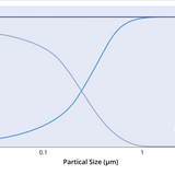 HEPA Filter Size Chart
High Efficiency Particulate Air (HEPA) filters are designed to efficiently remove airborne particles and contaminants, making them indispensable tools in laboratories and cleanroom facilities.
Read more... ULPA vs HEPA Filters: Which One is Right for You?
Ultra-Low Particulate Air (ULPA) and High-Efficiency Particulate Air (HEPA) filters are both used in laminar flow hoods to remove particles from incoming air.
Read more...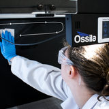 Laminar Flow Hood Cleaning Procedure
Regular and thorough cleaning of your laminar flow hood allows you to reliably conduct your experiments without risk of contamination.
Read more... UV Sterilization
Ultraviolet (UV) sterilization is a disinfecting technique that uses UV light to kill or damage microorganisms, such as bacteria, viruses, and fungi.
Read more... Air Flow in Laminar Flow Hoods
Laminar flow must be achieved to guarantee air flow will move in a single direction and ensure optimal performance of the hood. This is needed to achieve the clean air functions listed above.
Read more...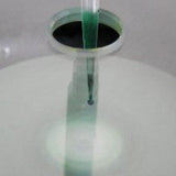 Spin Coating: Complete Guide to Theory and Techniques
Spin coating is a common technique for applying thin films to substrates. When a solution of a material and a solvent is spun at high speeds, the centripetal force and the surface tension of the liquid together create an even covering.
Read more... Which Spin Coater Features Do I Need?
Depending on your application and scale of film production, these features can be both beneficial and damaging to your final films. Before investing in a new spin coater, it is crucial to consider the different features and specifications available in the market.
Read more... How to Spin Coat to the Very Edge of a Substrate
This video demonstrates the static dispense spin coating method using 45 degree angle to avoid touching the edge of the substrate whilst moving the ink.
Read more... Getting Started with the Ossila Spin Coater
Spin coating is a widely used and versatile technique for depositing materials onto substrates with accurate and controllable film thicknesses.
Read more...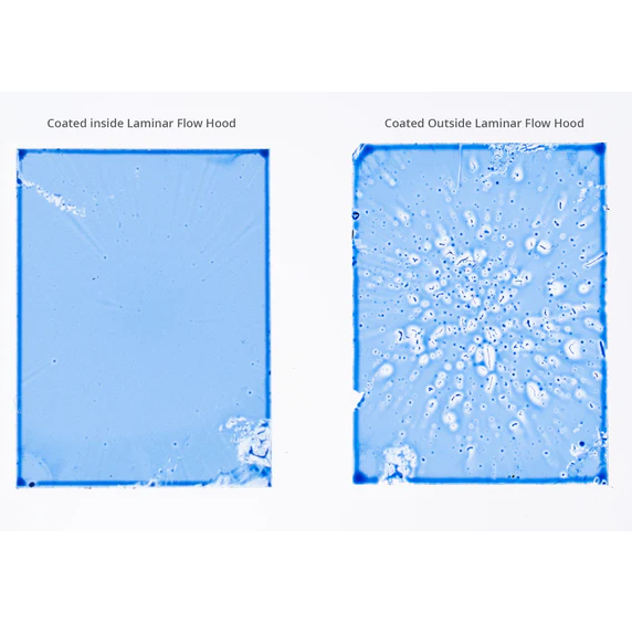 Spin Coating in Laminar Flow Hood
To achieve successful thin-film deposition via spin coating, it is crucial to minimize particle contamination. A vertical laminar flow hood can create a contamination free environment.
Read more... Video: How to Assemble the Vertical Laminar Flow Hood
Video guide on how to assemble the vertical laminar flow hood.
Read more... Video: How to Clean the Laminar Flow Hood
Video guide on how to clean your laminar flow hood.
Read more...Dip coating is a simple and effective technique which is commonly used in manufacturing across a wide range of different industries. Within research and development, it has become an important coating method for the fabrication of thin films using a purpose-built dip coater.
Read more... Getting Started with the Ossila Dip Coater
Dip coating is one of the most widely-used coating processes in industry and academia for producing thin films. To create a film, the substrate is first lowered into, and then withdrawn from, the solution.
Read more...Linear stages are used to achieve precise and controlled linear motion. They are integral to scientific research, the technology sector, industrial manufacturing, medicine, and more.
Read more... Do You Need a Linear Stage?
Whether you are involved in microscopy, spectroscopy, or metrology, a linear stage can be an invaluable tool. The decision to invest in a linear stage depends on the specific requirements of your application.
Read more... How to Choose a Linear Stage
Based on your research needs, there are key factors to consider when selecting a linear stage.
Read more... Types of Linear Stage
There are lots of different types of linear stages which vary in drive mechanism, axis, precision, and length. With this, linear stage motion can be implemented into a wider variety of applications.
Read more... How to Attach Your Linear Stage to a Breadboard
Learn how to attach your linear stage to a breadboard for stable, accurate motion control.
Read more... How to Assemble an XYZ Stage System
Learn how to combine your linear stages to create a multi-axis system.
Read more... Linear Sweep Voltammetry: Introduction and Applications
Linear sweep voltammetry (LSV) is a simple electrochemical technique. The method is similar to cyclic voltammetry, but rather than linearly cycling over the potential range in both directions, linear sweep voltammetry involves only a single linear sweep from the lower potential limit to the upper potential limit.
Read more...When it comes to depositing highly-uniform wet thin films, there are many different solution-processing techniques capable of producing high-quality films at low cost.
Read more... Contact Angle: A Guide to Theory and Measurement
This guide will explain what a contact angle is and how it is measured. It will also show you how the Ossila Contact Angle Goniometer works and how to get the best measurement results.
Read more... What is Surface Energy? Formula & Definition
Surface free energy is a measure of the excess energy present at the surface of a material, in comparison to at its bulk. It can be used to describe wetting and adhesion between materials.
Read more... UV Ozone Theory and Application
UV ozone cleaning is a photo-sensitized oxidation process in which organic molecules in their excited state chemically react with ozone molecules, resulting in the cleaving of bonds and the dissociation of molecules from the surface.
Read more...Surface wetting occurs when a droplet spreads out over a surface, such that its contact angle is below 90°. When the droplet spreads out completely, this angle will be 0°, and 'complete wetting' will have occurred.
Read more... Contact Angle Goniometer Applications
A contact angle goniometer is an instrument that measures the contact angle of a droplet on a surface. This is a useful, indirect measurement of surface wetting.
Read more...In this guide we will use the Ossila Contact Angle software to measure a droplet on an uneven surface.
Read more... How to Measure Surface Tension with the Goniometer
Video guide to measure the surface tension of a droplet.
Read more...Video guide to measure the contact angles of droplets on a surface.
Read more... How to Set Up and Use the Ossila Syringe Pump
With no external dependencies, the Ossila Syringe Pump is quick and easy to set up and use.
Read more... Getting Started With a Laboratory Syringe Pump
Understanding the fundamentals of syringe pumps is essential for their effective use, maintenance, and troubleshooting.
Read more... Syringe Pumps Explained: Types of Syringe Pump
Syringe pumps, or syringe drivers, are motorised devices that accurately control the movement of a fluid from a syringe by mechanically inserting or retracting the plunger. Syringe pumps feature stepper motors which can accurately move a platform attached to the plunger of a syringe.
Read more... Key Features of Ossila Syringe Pumps
Syringe pumps are commonly used in scientific research for precise and controlled delivery of fluids during experiments. They can be utilised for various applications in chemistry, biology, biochemistry, pharmaceuticals, and medical research.
Read more... How do Syringe Pumps Work?
Syringe pumps are electromechanical devices which are designed to convert rotational motion to linear motion. This linear motion can then be used to drive the plunger of a syringe and deliver a precise amount of solution.
Read more... Syringe Pump Flow Rate
The flow rate for a syringe pump refers to the rate at which a fluid is dispensed or withdrawn from a syringe using a syringe pump. It is typically measured in volume per unit of time.
Read more...Syringe pumps provide precise control over the movement and delivery of fluids and can be incorporated into a wide range of experimental setups to ensure that any work done is reproducible and accurate.
Read more...When auto dispensing solvents, droplets are sometimes dispensed after the syringe pump has stopped. The cause of solution dripping can be due to several factors.
Read more... What is a Spectrometer? Types and Uses
A spectrometer is a device that measures a continuous, non-discrete physical characteristic by first separating it into a spectrum of its constituent components.
Read more... How Does a Spectrometer Work? Principles Explained
Optical spectrometers take light and separate it by wavelength to create a spectra which shows the relative intensity of each. This basic principle has a wide range of applications and uses.
Read more...Spectrometers can be designed and built using a number of different optical configurations. Careful choice of components and configuration can avoid aberrations, which result in distorted or blurred spectra.
Read more... UV-Vis Spectroscopy Troubleshooting
It can be incredibly frustrating if you encounter a problem while performing UV-Vis spectroscopy, and usually causes an unnecessary delay.
Read more...Like any analytical technique, spectrometers are subject to error, including dark noise, stray light, and spectral bandwidth.
Read more...When an electron is excited into a higher energy state, either through absorption of a photon or another excitation method, this creates a positively charged space in the lower energy leel known as a "hole."
Read more... The AM1.5 Spectrum
Solar irradiance varies depending on where you are in the world. This is because of a combination of local atmospheric conditions and geometric considerations.
Read more...The purpose of a solar simulator is to recreate the sunlight received on Earth. This is easier said than done as sunlight starts its journey in complex nuclear reactions in the sun's core, and is modified on it's journey to us through interactions with the Earth's atmosphere.
Read more... Solar Simulator Applications
A solar simulator accurately and consistently mimicks solar radiation. The light from a solar simulator aims to reproduce a standard solar spectrum (usually AM1.5G).
Read more...Light can be measured either photometrically (only light visible to the human eye is considered) or radiometrically (also considers the energy in the invisible parts of the electromagnetic spectrum).
Read more...New developments in solar cell technology have enabled the realisation of flexible solar cells, the applications of which can be utilized in more imaginative ways than ever before.
Read more...A solar simulator has several components that help to simulate the solar spectrum uniformly for a defined test area. The most important part of the several components is the light source, however the other components ensure the light source outputs the solar spectrum correctly.
Read more... How to Set Up a Solar Simulator Light Source
The solar simulator light source is compact, lightweight and can be easily installed in any lab using adjustable height stand provided with it.
Read more... Automated Solar Simulator Assembly
This system was designed to be easy to use, and effortless to assemble. This video and subsequent guide will demonstrate how easy setting up your testing lab can be with the Ossila Automated Solar Cell Testing Bundle.
Read more... How to Assemble the Automated Solar Cell Testing Kit: Video Guide
An easy step-by-step guide to assembling the automated solar cell testing kit.
Read more... How to Check Solar Simulator Calibration
It is important to ensure that your solar simulator is outputting a consistent spectral output. Different solar simulators will have different bulb lifetimes.
Read more... Solar Simulator Classification and Calibration
Solar simulators must be evaluated according to one of the three standards, and comply with the specifications set out within.
Read more... Solar Simulator Irradiance and Spectral Mismatch
Solar simulators generally attempt to replicate the standard AM1.5G spectrum which has a total integrated irradiance of 1000.4 W/m2 over the wavelength range of 280 nm – 4000 nm.
Read more... Solar Cell Testing & Characterization
One main application of solar simulators is to test solar cell devices and modules. To characterise how solar cells will perform in the real world, it is vital that you use a solar source that mimics the suns spectrum well. You could of course use actual sunlight, but this is an uncontrollable variable.
Read more... Measuring J-V Curves with Ossila Solar Cell Testing Equipment
When it comes to testing the performance of solar cells, accurate measurements and reliable equipment are essential. If you are conducting research into PV materials, understanding how to measure and interpret J-V curves is crucial in assessing device performance
Read more... Analyzing and Improving Low Device Metrics: FF, VOC and JSC
Anaylzing key device metrics such as fill factor (FF), open-circuit voltage (VOC), and power conversion efficiency (PCE), can help you find potential issues with your solar cell devices
Read more... Solar Simulator Light Sources
Choosing the right light source for your solar simulator is one the most important decisions to make when setting up a PV testing laboratory
Read more... How To Write A Research Paper
A research paper is an academic document that involves analysis, interpretation, and argumentation derived from independent research. Unlike academic essays, research papers tend to be lengthier and more intricate, assessing both writing proficiency and scholarly research abilities. Crafting a research paper entails showcasing a deep understanding of the topic, interacting with diverse sources, and offering an original perspective to the discourse. Our guide will guide you through writing individual sections from abstract to conclusion.
Read more... How To Give A Great Presentation
In the world of science, sharing your research findings is significant. Whether you are talking about it in person, putting up a poster, or writing it down, getting the word out is important for moving science forward and getting people talking.
Read more... Optical Spectroscopy
Optical spectroscopy (or UV-Vis spectroscopy) is a versatile and non-invasive technique that can be used to study a wide range of materials.
Read more... Light Sources for Spectroscopy
Spectroscopy can be performed using a range of different light sources. These can typically be categorised as being either monochromatic or broadband.
Read more... Jablonski Diagrams
Jablonski diagrams are the simplest way to the transitions between electronic and vibrational states. The representative energy levels are arranged with energy on the vertical axis and vary horizontally according to energy state multiplicity.
Read more... Python for Spectroscopy | Spectra Data Visualization
Optical spectroscopy data can be processed faster and more consistently using programming tools such as Python. This is a step-by-step guide of how researchers process multiple spectra that were taken using the Ossila Optical Spectrometer. The code in this guide is designed for the Ossila Optical Spectrometer.
Read more...Data can be easily plotted using the following Python code to plot data using Pandas DataFrame.Just copy and paste the code below into your Python virtual environment and start plotting.
Read more...Spectroscopy is an invaluable technique used to study the interaction between radiative energy and matter. Different types of radiative energy used in spectroscopy include electrons, neutrons, ions, and acoustic waves.
Read more... History of Spectroscopy
The history of spectroscopy is a rarely told story, though it is a fascinating one that has profoundly shaped modern science. The research spans three centuries. This history takes us from age-old curiosities over the nature of light, to discoveries about the solar system and chemical elements and their structures.
Read more...The Beer-Lambert Law is a fundamental principle in spectroscopy. Optical spectrometers can quantify the absorption of light by a sample. Using the Beer-Lambert law, you can use these absorbance measurements to easily measure and monitor the concentration of different materials within a solution.
Read more... Fluorescence and Phosphorescence
Both fluorescence and phosphorescence are types of photoluminescence. Photoluminescence refers to radiative emissions where the absorbance of a photon is followed by the emission of a lower energy photon. The main empirical difference between fluorescence and phosphorescence is the time in between absorbance and the emission of photons.
Read more...The blazed diffraction grating is a type of grating that has a "sawtooth" profile. Blazed diffraction gratings will maximise the grating efficiency in one desired diffraction order at a specific wavelength, while other orders are minimised.
Read more... Thin Film Spectroscopy: Setup and Measurement
This article contains some advice from our researchers that should help you get started taking optical spectroscopy measurements of thin films.
Read more... Measuring Thin Film Fluorescence
To measure the fluorescence of a thin film, you will need an optical spectrometer, a fixed sample holder and a high energy light source (such as a UV laser or the Ossila UV light source). We also recommend using optical fiber cables between modular elements to reduce the attenuation of your signal.
Read more...Optical fibers (or fiber optic cables) are cables which transmit light efficiently along an extremely thin glass (silica) or plastic fiber. Light travels down the cable due to total internal reflection.
Read more...Electroluminescence (EL) is the generation of light through the radiative recombination of holes and electrons which have been injected into the material from cathode and anode contacts. The charge carriers are injected into the material due to an applied bias over the cathode and anode. These cathode and anodes are orientated opposite each other.
Read more...The different types of spectroscopy can be categorised by either the application it is used for or by type of radiative energy employed. The application of spectroscopic methods in organic (carbon-based) chemistry and organic electronics is known as organic spectroscopy.
Read more... Absorption Spectroscopy
In absorption spectroscopy, the intensity of light absorbed by a sample is measured as a function of wavelength. This can provide important information about the electronic structure of an atom or molecule.
Read more...You should not be measuring negative absorbance values for any sample. Absorbance measurements come from transmission measurements where light that passes through your sample is collected by the spectrometer (or spectrophotometer) and compared to a reference spectrum.
Read more...Photoluminescence is luminescence resulting from photoexcitation. In other words, photoluminescence is when a material emits light following the absorption of energy from incident light from another light source.
Read more...Kasha's rule states that photon emission (fluorescence or phosphorescence) only happens from the lowest-energy excited electronic state of a photoactive molecule.
Read more... Measuring BODIPY Fluorescence with UV Vis Spectroscopy
BODIPY is an organic fluorophore with impressive fluorescent quantum yield, small stokes shift and impressive chemical and photostability. These are often used in biological labelling and as an organic fluorescent dye.
Read more...Photoluminescence quantum yield (PLQY) is a measure of the efficiency of photoluminescence in a system. It compares the number of photons emitted to the number of photons that have been absorbed.
Read more... Sample Preparation for UV-Vis Spectroscopy
When done correctly, UV-Vis (or optical) spectroscopy can be a powerful technique which can reveal intricate details about the molecular structure and optical properties of a sample. However, without well prepared samples, the results can be not only challenging to interpret but also potentially deceptive.
Read more...Photoluminescence occurs when electrons relax from photoexcited states radiatively. Emissions resulting from singlet-singlet transitions are known as fluorescence. However, there are a number of ways in which electrons in these excited states can relax non-radiatively.
Read more...Thermally Activated Delayed Fluorescence (TADF) is a mechanism by which triplet state electrons can be harvested to generate fluorescence.
Read more...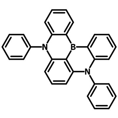 Multi-Resonance Thermally Activated Delayed Fluorescence (MR-TADF)
Multiple resonance thermally activated delayed fluorescence (MR-TADF) is a light emitting process engaging the same working principle as thermally activated delayed fluorescence (TADF).
Read more... Molecular Design Principles of MR-TADF Materials
The design of multiple resonance thermally activated delayed fluorescent (MR-TADF) materials requires careful selection of molecular scaffolds and substituents to achieve the desired photophysical properties i.e. color and color purity.
Read more... MR-TADF Applications
MR-TADF emitters show great application potential in high color purity and high-resolution organic light-emitting diode (OLED) displays, and their long emission lifetimes also make them ideal for use in bioimaging probes, fluorescent sensors, and phototheranostics.
Read more... TADF Exciplex OLED Technology
A thermally activated delayed fluorescence (TADF) exciplex is an excited-state species that can exhibit thermally activated delayed fluorescence or transfer its energy to a lower-energy emitter. TADF exciplex is formed between electron-donating and electron-accepting molecules by intermolecular charge transfer.
Read more... TADF Blue OLED Emitters
TAmong the various challenges faced in the development of organic light-emitting diodes (OLEDs), the quest for a highly efficient and stable blue emitter has remained to be one of the most difficult.
Read more...Triplet-triplet annihilation (TTA) is an energy transfer process where two molecules in their triplet excited state interact to produce two singlet states: one molecule transitions to its singlet excited state and one molecule transitions to its singlet ground state
Read more...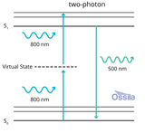 Two-Photon Absorption and Upconversion
Two-photon absorption (TPA or 2PA) is a nonlinear optical process in which a material absorbs two photons simultaneously (or within a very short timespan) to excite an electron from a lower-energy state to a higher-energy state. The total energy of the two photons is equal to the energy difference between the two states.
Read more...Intramolecular charge transfer (ICT) refers to the transfer of charge within a single molecule (intra = “within” in Latin). In molecules containing one or more electron donor and acceptor groups, ICT can occur if the molecule is in an excited state.
Read more... What is a Fluorophore?
A fluorophore is a chemical compound that is fluorescent, meaning it emits strong glowing colours. There are three key groups of chemical compounds that can fluoresce:
Read more...A chromophore is a molecule or section of a larger compound that absorbs and reflects specific electromagnetic radiation. Any visible light that is reflected by the molecule is observed as colour.
Read more... What is a Photosensitizer?
A photosensitizer is a molecule that absorbs light and converts it to a different form of energy. This energy is typically transferred to other molecules through an energy transfer mechanism, such as Förster or Dexter transfer.
Read more...An exciplex (or excited complex) is a complex formed between two different conjugated molecules (monomers), one of which is in an excited state.
Read more...Conductivity, resistivity, resistance and sheet resistance are all electrical quantities that describe a material or an electrical component’s opposition to electrical current flow.
Read more...This guide explains the theory behind sheet resistance, an electrical property of thin films of materials, and demonstrates how the four-probe method can be used to measure it.
Read more... How to Measure Sheet Resistance using a Four-Point Probe
This guide gives an overview of how to use the Ossila Four-Point Probe System, as well as some general tips and tricks for measuring sheet resistance.
Read more... Video: How to Replace the Four-Point Probe Head
A video guide on how to replace the Ossila Four-Point Probe Head.
Read more...Slot-die coating is an extremely versatile deposition technique in which a solution is delivered onto a substrate via a narrow slot positioned close to the surface.
Read more... Getting Started with the Ossila Slot Die Coater
Compatible with both roll-to-roll and sheet-to-sheet deposition processes, slot die coating is one of the best techniques available for scalable thin film deposition.
Read more... Solar Cells: A Guide to Theory and Measurement
A solar cell is a device that converts light into electricity via the photovoltaic effect.
Read more... History of Solar Cells
Humans have been using solar energy for light and heat for hundreds of years. Chinese, Greek, and Roman inventors built structures that tracked the sun to capture light and warmth. Later, concentrated light was applied to ignite fires using curved metallic objects known as 'burning mirrors'. By the 18th century, natural philosophers were trapping solar heat with glass.
Read more...The global demand for electricity is continuously increasing. More and more resources are being invested into finding new energy sources rather than relying on our finite fossil fuel supply. One of these sources is sunlight.
Read more...One of the factors preventing widespread adoption of solar panels is the limited space for installation, particularly in densely populated areas like cities where land and roof space are scarce. To address this issue, transparent solar panels are being introduced as a potential solution to capture solar energy in more areas.
Read more... Do Solar Panels Work at Night?
Solar panels are not able to generate electricity during the night. Solar panels work by absorbing photons of visible light and converting this to electricity. Of course, at night, there is no sunlight for solar panels to absorb.
Read more...A common concern amongst home and business owners is whether solar panels can work efficiently in the climate they operate in. Solar panels are more efficient the more sunlight is incident on them.
Read more... Monocrystalline vs Polycrystalline Solar Panels
The rise in popularity of solar panels has resulted in several types of solar panels being developed. Each uses slightly different materials or technology to achieve the same goal: convert the sun’s energy into useable electricity. Of these, monocrystalline and polycrystalline solar panels are by far the most popular choices.
Read more... How Is Solar Energy Stored?
Solar panels harness the free and renewable energy produced by the sun to generate electricity. While they have many advantages, they face a significant drawback: they're unable to produce electricity without sunlight. Consequently, energy production is reduced and reliability suffers at night or during long periods of poor weather.
Read more...PTAA and Spiro-OMeTAD are both used as hole transport layers in high efficiency perovskite solar cells (PSCs). Regular architecture devices using PTAA and Spiro-OMeTAD layers have demonstrated power conversion efficiencies (PCEs) of over 22% and 25% respectively.
Read more...An I-V curve (short for 'current-voltage characteristic curve'), is a graphical representation of the relationship between the voltage applied across an electrical device and the current flowing through it.
Read more... What is Voltammetry? Types and Applications
Voltammetry is the study of the current response of a chemical under an applied potential difference. Voltammetry encompasses a number of different methods.
Read more... Organic Photovoltaics: An Introduction
Organic photovoltaics (OPVs) have received widespread attention due to promising qualities, such as solution processability, tunable electronic properties, low temperature manufacture, and cheap and light materials.
Read more...Due to their high efficiency and well-established manufacture, crystalline silicon (c-Si) solar cells currently dominate the solar cell market.
Read more...Whilst the majority of commercial solar cells are currently made using crystalline silicon (c-Si), thin-film alternatives have the potential to be cheaper, flexible, and more straightforward to produce.
Read more... OLED Fabrication Guide
In this guide, we demonstrate how to make standard OLED devices in a glove box using materials and equipment easily available to any lab. Find out more.
Read more...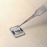 Organic Solar Cell Fabrication Guide
This guide demonstrates how to fabricate standard organic solar cells (OSCs) using materials and equipment that are readily available. Find out more.
Read more...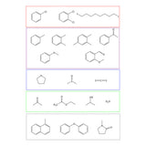 Green Solvents for Organic Photovoltaics
Whilst efficiencies of lab-scale organic photovoltaic (OPV) cells have continued to rise in recent years, the majority of systems use aromatic halogenated solvents to dissolve the active layer.
Read more... What is Molecular Engineering?
Molecular engineering is simply the design and synthesis of molecules with specific properties and functions in mind. Certain chemical groups and atoms incorporated into molecules results in them having certain characteristics.
Read more...Molecular electronics or "moletronics" is to use molecules as building blocks to create electronic components. These molecular electronic components include transistors, diodes, capacitors, insulators, and wires.
Read more... PEDOT:PSS Conductive Polymer
PEDOT:PSS is a blend of two distinct polymers: poly(3,4-ethylenedioxythiophene) (PEDOT) and polystyrene sulfonate (PSS).
Read more...Poly(3,4-ethylenedioxythiophene), referred to as PEDOT, is an intrinsically conducting polymer (ICP), defined as being composed of macromolecules with conjugated sequences of double bonds along its chains.
Read more...PEDOT synthesis involves the oxidative chemical or electrochemical polymerization of EDOT monomer.
Read more...PEDOT:PSS has conductivities in the range of 10-4 - 103 S cm-1. PEDOT:PSS is conductive because it contains the conjugated intrinsically conductive polymer (ICP) PEDOT.
Read more...PEDOT:PSS work function ranges 4.8 - 5.2 eV for commercially available products.
Read more... PEDOT:PSS in Solar Cells
PEDOT:PSS layers are often used in third generation photovoltaics like organic or perovskite solar cells. It is an attractive material for these applications due to its:
Read more... PEDOT:PSS Electrodes
The choice of electrode is very important in many optoelectronic devices. Solar cells, LEDs and photodetectors all need an electrode on either side of the device. These electrodes should meet the following criteria.
Read more...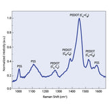 PEDOT:PSS Characterization using Raman Spectroscopy
The characterization of PEDOT:PSS is essential for determining the relationship between the materials structure, morphology and resulting properties. This is particularly important for their application in electronic devices where their electronic and optical properties are crucial in determining device performance.
Read more...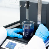 PEDOT Coating and Solution Processing
Methods for depositing PEDOT:PSS, are crucial for fabricating various organic electronic devices. These methods play a significant role in determining the film thickness and morphology, electrical properties, and performance of PEDOT-based materials.
Read more... PEDOT:PSS Applications
PEDOT:PSS stands out as a promising conductive polymer due to its large range of conductivities, transparency, flexibility, and ease of processing.
Read more...Two commonly used materials for hole selective layer (HSL) or hole transport layer (HTL) are PEDOT:PSS (poly(3,4-ethylenedioxythiophene) polystyrene sulfonate) and self-assembled monolayers (SAMs). Each offers distinct advantages and limitations that impact their effectiveness in solar cells.
Read more... Solar Cell Encapsulation in a Glove Box
When working with air sensitive compounds, it is vital that to protect your materials before removing them from inert atmospheres (like a glove box). One way to do this is to encapsulate your devices before exposing them to ambient conditions.
Read more...The rapid improvement of perovskite solar cells has made them the rising star of the photovoltaics world and of huge interest to the academic community.
Read more... History and Evolution of Perovskites
The discovery of perovskite crystals in the Ural Mountains in the 19th century was followed by the discovery of metal halide perovskites some 50 years later.
Read more...Wide bandgap (WBG) perovskites are a subset of perovskite semiconductor materials. These perovskite materials are characterized by a bandgap energy (Eg) >1.7 eV.
Read more...Narrow bandgap (NBG) perovskites are a subclass of perovskite materials, and loosely refers to the ones with bandgaps less than 1.4 eV. Tin-based perovskites (containing iodide anion) are often have a narrow bandgap.
Read more...Methylammonium lead iodide (MAPbI3) was one of the first perovskite materials used in perovskite solar cells. These crystal structures combine the organic A cation methylammonium (MA+, CH3NH3+) and divalent lead (Pb+) with three iodide anions (I-).
Read more...Formamidinum lead iodide (FAPbI3) is a material used for perovskite solar cells. FAPbI3 was introduced in 2014 as an alternative to MAPbI3 (Eperon 2014).
Read more... Perovskite Fabrication
This guide describes our recommended fabrication routine for perovskite solar cells using Ossila I101 Perovskite Precursor Ink which is designed to be used with a bottom ITO/PEDOT:PSS anode and a top PC70BM/Ca/Al cathode.
Read more...Instructions for how to fabricating perovskite solar cells with the following architecture: SnO2/perovskite materials/Spiro-OMeTAD (sublimed)/Au Solar Devices
Read more...As part of our photovoltaic substrate system, Ossila offers patterned Indium Tin Oxide (ITO) substrates which are designed to work with our evaporation masks to create multi pixel devices.
Read more...This article aims to introduce some methods that have been adapted to improve perovskite solar cell stability.
Read more...Perovskite solar cells show impressive efficiencies and offer “a different kind of solar cell” that could be cheap to manufacture and could be semi-transparent, lightweight, and flexible.
Read more...2D perovskites are perovskite materials with a layered crystal structure. They are made up of metal-halide sheets, separated by large organic cations called spacers.
Read more...Perovskite solar cells have demonstrated impressive device metrics, including open-circuit voltages of up to 1.2V. However, in order for PSCs to achieve their theoretical best efficiencies, all non-essential recombination pathways should be eliminated.
Read more... I301 Triple Cation Perovskite Solar Cells Processing
A condensed summary of our fabrication routine for standard architecture devices using our I301 Triple Cation Perovskite Precursor Ink. This recipe is based on the one described by Saliba et al (2018).
Read more... Perovskite FAQ
Our technical support team receive enquiries about perovskite solar cell or photovoltaic fabrication on a regular basis. For your convenience, we've collated some of the most common questions here which you may find helpful when using I101 or I201 perovskite precursor inks.
Read more...Self-assembled monolayers (SAM) are well-organised, one molecule thick layers that form on a solid surface. SAM molecules adsorb on a substrate via chemical or physical bonds. They spontaneously organize themselves into ordered structures on the substrate.
Read more... Deposition of Self-Assembled Monolayers
Self-assembled monolayers (SAMs) are well-organized one molecule thick layers that spontaneously form on a surface. They have a high potential for use in a wide range of applications due to their well-defined structure and properties.
Read more... Applications of Self-Assembled Monolayers
Self-assembled monolayers (SAMs) are highly organized single layers of molecules that form on a surface. This is driven by the chemisorption of specific functional groups on the SAM molecules that have a strong affinity for a particular surface.
Read more...Self-assembled monolayers (SAMs) provide a versatile and cost-effective method for surface modification and the creation of molecular-scale electronic devices. By selecting the appropriate head, spacer and tail group for the SAM molecules the following properties can be adjusted:
Read more...Incorporating self-assembled monolayers (SAMs) within perovskite solar cells has improved device efficiency. SAMs exist as ultrathin layers that can be engineered to improve various aspects of the solar cell including charge transport and stability. SAMs have benefits including:
Read more... Introduction to 2D Materials
The foundation of technology is the understanding of material systems. Specific material properties are required depending on the application.
Read more... Carbon Nanotubes: Uses, Properties and Limitations
Carbon nanotubes (CNTs) have been deemed a wonder material due to their remarkable and highly unique physical and chemical properties. They have received much attention over the past decade as a promising material, particularly in the trending field of nanotechnology.
Read more... What are Multi-Walled Carbon Nanotubes?
Multi-walled carbon nanotubes (MWCNTs) consist of multiple carbon nanotubes nested within one another. The carbon nanotubes are just one atom thick and this gives MWCNTs unique electrical and mechanical properties.
Read more... What are Single-Walled Carbon Nanotubes (SWCNT)?
Single-walled carbon nanotubes (SWCNTs) are sheets of graphene that have been rolled up to form a long hollow tube, with wall thickness of a single atom. Their one-dimensional structure gives them extraordinary mechanical, electrical and thermal properties.
Learn more... The Properties of Carbon Nanotubes
Carbon nanotubes (CNTs) have unique properties such as high conductivity and strength. They have similar properties to another carbon allotrope known as graphene. This is due to the similarity in structure of 2D sheet-like graphene and 1D carbon nanotubes which are essentially cylindrical tubes of rolled up graphene.
Learn more... How are Carbon Nanotubes Made?
There are multiple methods for producing carbon nanotubes (CNTs) and they usually involve gas phase processing. The three key methods are; chemical vapour deposition (CVD), laser ablation and arc discharge.
Learn more... The Different Types of Carbon Nanotubes
The two main types of carbon nanotubes are single-walled carbon nanotubes (SWCNT) and multi-walled carbon nanotubes (MWCNT). Scientific research has led to the development of other types of carbon nanotubes with distinct features. Modifications to the chemistry and structure of carbon nanotubes have improved specific properties for various applications.
Learn more... What is the Difference Between SWCNT and MWCNT?
Single-walled carbon nanotubes (SWCNTs) and multi-walled carbon nanotubes (MWCNTs) have some similarities and some key differences. Both materials are made from hexagonal lattices of carbon, specifically graphene sheets rolled up to form tubular structures. However, the nested structure of MWCNTs gives them distinct properties that differentiate them from SWCNTs.
Learn more... What is a Carbon Nanotube Battery?
Carbon nanotubes (CNTs), such as single-walled carbon nanotubes (SWCNT), have been tipped as one of the most exciting nanomaterials in the development of battery technology. The key properties of CNTs that make them ideal candidates as battery components is their high electron conductivity, high strength and lightweight nature.
Learn more... Carbon Nanotubes vs Graphene: Structure, Properties and Uses
Carbon nanotubes (CNTs) and graphene are two ground-breaking nanomaterials composed entirely of carbon atoms. Both are allotropes of carbon where atoms are bonded in a hexagonal lattice.
Learn more... Properties of Fullerene
Fullerene C60 exhibits unique structural, chemical, electronic, and thermal properties. This is due to its highly symmetrical icosahedral structure that contains a mixture of single and double bonds. All fullerenes have partial electron sharing across the molecule and a high affinity for electrons.
Read more... What are Fullerenes?
Fullerenes are an allotrope of carbon and are known for their hollow, cage-like structures. They are composed entirely of carbon atoms that form closed, convex polyhedra. The atoms are bonded together to form hexagonal and pentagonal rings, like the pattern found on a soccer ball or geodesic dome.
Read more...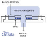 How are fullerenes made?
Today, fullerenes are made using three main methods; Huffman-Krätschmer, combustion and microwave. Chemical synthesis techniques, such as laser irradiation and pyrolysis, offer exciting possibilities for producing fullerene derivatives that were previously not accessible.
Read more... Viscoelastic Transfer of 2D Material Using PDMS
Viscoelastic transfer using polydimethylsiloxane (PDMS) stamps is one of the methods used for the deterministic placement of 2D materials and the fabrication of van der Waals heterostructures.
Read more... Uses of Fullerene and its Derivatives
Fullerene and its derivatives are used in chemical, electronic, medicinal, and biological sciences due to their unique physical and chemical properties. Fullerene, also known as C60 or buckminsterfullerene, is a type of carbon allotrope that has properties that can be tuned depending on what it will be used for.
Read more... Water-Soluble Fullerenes: Preparation and Applications
Water-soluble fullerenes, such as fullerenol C60, are either chemically modified, polymer grafted, or encapsulated in a hydrophillic agent. Fullerenes can then disperse or solubilize in aqueous media.
Read more... Polymer-Fullerene Bulk Heterojunction Solar Cells
Polymer-fullerene bulk heterojunction (BHJ) solar cells are based on blends of semiconducting polymers and fullerene derivatives, such as PCBM. It is described as a bulk heterojunction as it involves a blend of two materials with differing energy band gaps, forming a dispersed, interpenetrating network.
Read more... Molybdenum Disulfide
Molybdenum disulfide belongs to a class of materials called 'transition metal dichalcogenides'. Materials in this class have the chemical formula MX2, where M is a transition metal atom and X is a chalcogen.
Read more... Reducing Graphene Oxide to Graphene Using Environmentally Safe Materials
Graphene has many potential electronic, optoelectronic and biological uses. However, graphene itself is non-soluble, and this makes it very difficult to deposit from solution.
Read more... What is Graphene?
Graphene is a hexagonal lattice of carbon atoms that connect to form a single sheet in 2 dimensions.
Read more...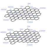 What is Graphene Oxide?
Graphene oxide (GO) is a two-dimensional material with oxygen-functionalized surfaces, derived from graphite.
Read more... Graphene Batteries
Graphene batteries are advanced energy storage devices. Graphene materials are two-dimensional and are typically made solely of carbon.
Read more... Graphene vs Graphite
Graphene is a single layer of carbon atoms arranged in a hexagonal pattern, like a sheet of paper. Graphite, on the other hand, is made up of many layers of graphene stacked on top of each other, like a stack of paper.
Read more... Graphene Properties and Applications
Graphene materials have ultrahigh surface area, high strength, and exceptional conductivity making them highly valuable for various applications. Its large surface area enhances energy storage, sensor sensitivity, and water purification efficiency.
Read more... Hexagonal Boron Nitride Structure
Hexagonal boron nitride (h-BN) has a layered structure. In a layer of h-BN, each boron atom is covalently bonded to three nitrogen atoms and vice versa.
Read more... Hexagonal Boron Nitride Properties
The properties of bulk hexagonal boron nitride crystals differ from that of the monolayer material. The bulk exists as layered hexagonal lattice material similar to graphite.
Read more...Tungsten disulfide (WS2) exits in different forms, each with their own beneficial properties. Bulk WS2 offers advantages such as exceptional lubricity and high thermal stability.
Read more... An Introduction to Batteries
Typically, batteries work by a process known as intercalation. This process occurs across the battery components. Most batteries consist of the same components.
Read more...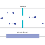 Lithium-Ion Battery Components and Working Principle
Lithium-ion batteries operate based on electrochemical reactions, specifically redox reactions involving lithium and sometimes other redox-active elements. These reactions result in the movement of lithium ions between the electrodes and the flow of electrons through an external circuit.
Read more...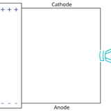 Cathode vs Anode: What is the Difference?
Defining a cathode and anode as positive and negative, or as the source and sink of a current, depends on your definition of current itself. Current can describe the flow of positive or negative charge.
Read more... Graphene Battery vs Lithium-Ion Battery
This page discusses the pros and cons of Lithium-ion (Li-ion) batteries and graphene batteries and the future outlook for battery research.
Learn more...Lithium-ion (Li-ion) batteries can catch fire due to a process known as thermal runaway, which is triggered by various factors and involves a series of heat-releasing reactions. While Li-ion batteries are widely used in laptops, cameras, and electric vehicles (EVs) such as scooters and cars, their rise in popularity has not been without issues. In the UK alone, fire services responded to 921 lithium-ion battery fires in 2023, a 46% increase from the previous year.
Learn more... What is a Battery C-Rate?
C-rate refers to the rate at which a battery charges or discharges relative to its maximum capacity. In other words, the speed at which delithiation and lithiation occurs in a lithium-ion battery. The higher the C-rate the faster charging or discharging occurs.
Learn more...An LFP battery gets its name from it’s key material component, lithium iron phosphate powder, which has the chemical formula LiFePO4. It is also known as lithium ferro phosphate which gets shortened to LFP, hence the name.
Learn more...LMFP stands for lithium manganese iron phosphate, a material used in the cathode of lithium-ion batteries. With the molecular formula LiMnxFe(1-x)PO4 it has the same crystal structure type as lithium iron phosphate (LFP), another popular cathode material.
Learn more...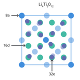 What is an LTO Battery?
An LTO battery is named after its key component, lithium titanium oxide (LTO) powder. The material is also referred to as lithium titanate with the chemical formula Li4Ti5O12. Unlike most lithium-ion battery materials it is used as the anode active material.
Learn more...The NCA battery gets its name from the cathode active material, lithium nickel cobalt aluminum oxide (LiNixCoyAlzO2, where x+y+z=1) which gets shortened to nickel cobalt aluminum (NCA). NCA is the cathode active material with a specific ratio of metals.
Learn more... How Do Rechargeable Batteries Work
Batteries can be recharged by plugging them into a power source, which initiates electrochemical reactions causing charged species within the battery to return to the anode. Restoring the battery’s potential energy.
Read more...A solid electrolyte interphase (SEI) forms on the negative electrode in lithium-ion batteries (LIBs) due to the decomposition of electrolyte. The decomposition by-products build up on the surface of the anode and form an independent phase of material, different to the electrode and electrolyte.
Read more...A hybrid energy storage system (HESS) is defined by the combination of two or more energy storage technologies within one operating system. This helps combine the benefits of the different technologies as well as resolve the issues faced by the individual energy storage solutions.
Read more...A solar battery is a battery energy storage system connected to solar panels. Electricity generated by converting sunlight into energy through solar panels can be stored in the battery for later use. Most solar batteries are lithium-ion, the same type used in electric vehicles, phones, and laptops.
Read more...Lithium plating is a mechanism of degradation in lithium-ion batteries (LIBs). It describes the accumulation of metallic lithium on the surface of the anode (usually graphite powder). Lithium ions gather at the anode surface and form metallic deposits.
Learn more...Lithium-polymer (LiPo) batteries are a type of lithium-ion battery technology that uses polymer electrolytes. This differs from standard lithium-ion batteries which use a solvent based electrolyte. Polymer electrolytes used are highly ionically conductive and form lithium-ion conduction channels.
Learn more...The state of charge (SoC) of a battery is defined as the ratio of remaining charge in the battery compared to the maximum charge capacity of the battery. It indicates how much energy remains in the battery and when it will need recharging.
Learn more...Solid-state batteries (SSBs) differ from conventional lithium-ion batteries (LIBs) in terms of both their components and fundamental design features. Instead of a liquid electrolyte, they use a solid electrolyte to conduct lithium ions between electrodes.
Learn more...A ternary lithium battery is a type of lithium-ion battery (LIB) that has a cathode composed of three different metals. The metals are nickel (Ni), cobalt (Co), manganese (Mn) or aluminium (Al).
Read more...Internal resistance of a battery is one indicator of a battery’s current-carrying capacity. There is an inverse relationship between the two parameters.
Learn more...Charge transfer resistance (Rct) is a major form of resistance within batteries that contributes to a reduction in efficiency. Rct is related to the activation barrier of electrochemical reactions.
Learn more...Power density vs energy density is an important consideration when it comes to battery science. Batteries that have high energy density, (can store a lot of energy) may not be able to deliver that energy quickly. Conversely batteries with high power density (can deliver a lot of power) may not be able to deliver that energy for a long period of time.
Learn more...Battery design and architecture plays a critical role in battery performance and lifespan. Batteries are made of two electrodes made of materials capable of redox reactions that are separated by an electronically insulating but ion conducting electrolyte. Spontaneous chemical reactions at the electrodes drive the movement of electrons through the external circuit and the migration of ions through the electrolyte.
Learn more...Conductive additives play a significant role in enhancing the performance of electrodes in batteries by improving their electrical conductivity. Many electrode materials that play an active role in the electrochemical reactions involved in energy storage have relatively poor intrinsic electrical conductivity.
Learn more...Battery binders are typically polymeric materials that are used like glue to hold together electrode components. Crucial for providing stability, they ensure even coatings and robust adhesion. Carefully selected electrochemical properties prevent unwanted chemical reactions with the active electrode materials. Importantly, they allow efficient electron and ion movement within the battery system.
Learn more... What are Advanced Ceramics?
Advanced ceramics are the next generation of ceramic materials. According to the 1993 Versailles project on Advanced Materials and Standards (VAMAS) an advanced ceramic material is defined as "an inorganic, non-metallic, basically crystalline material of rigorously controlled composition and manufactured with detailed regulation from highly refined and/or characterized raw materials giving precisely specified attributes".
Learn more... What are Transparent Conductive Oxides?
Transparent conductive oxides (TCOs) are metal oxides, such as zinc oxide and tin oxide, that are capable of conducting electricity whilst being optically transparent. This means they absorb a low number of electromagnetic waves within the visible region of the spectrum, appearing see-through.
Learn more... An Overview of Metal Oxide Nanoparticles
Metal oxide (MOx) nanoparticles (MONPs) are a class of nanomaterial with interesting and diverse chemical, optical, electrical and magnetic properties. Different metals bond to oxygen forming a variety of crystal structures under specific conditions. The shape and nanostructure of these materials effects their surfaces which in turn impacts the way they interact with light, electricity, magnetic fields and other materials.
Learn more...Transition metal oxides (TMOs) are compounds of transition metals bonded to oxygen. A transition metal is an element in the periodic table that has a partially filled d-shell or which forms cation with an incomplete d-shell. TMOs have been extensively researched due to their wide range of chemical and physical properties.
Learn more...Metal oxides are used as photocatalysts due to their ability to accelerate chemical reactions when exposed to light. Examples include zinc oxide (ZnO), iron oxide (Fe2O3), titanium dioxide (TiO2) which possess useful electronic structures, light absorption properties and charge transport characteristics suited to photocatalysis.
Learn more...Metal oxide semiconductors are comprised of positive metallic ions connected to negative oxygen ions via ionic bonds. Typically in solid form, they are non-stoichiometric compounds, which means their chemical formula cannot be exactly represented by a ratio of small natural numbers.
Learn more...Electrochromism describes the process of materials changing appearance in response to electricity. The components of the name, “electro” describes the need for electricity and “chromism” describes the involvement of color. Electrochemical oxidation and reduction reactions lead to changes in a material’s absorption characteristics in the UV-Vis-NIR region.
Learn more...The two main categories are organic materials such as small molecules and polymer and inorganic materials such as metal oxides and metal complexes. Electrochemical oxidation and reduction reactions lead to changes in a material’s absorption characteristics in the UV-Vis-NIR region. As a result, electrochromic materials experience reversible color changes.
Learn more...Metal oxides (mainly II-VI semiconductors) are used as sensors due to their low cost, ease of manufacture, quick response time, wide detection ranges and resistance to harsh conditions. Metal oxide sensors are versatile semiconducting devices that detect gases, chemicals, and biological analytes by converting surface interactions into measurable electrical signals.
Learn more... Solution Based OFETs
This guide describes the fabrication of evaporation-free OFETs using the Ossila pre-patterned ITO OFET substrates (product codes S161 & S162).
Read more...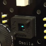 OLED Testing Guide
This guide gives you an overview of what to consider when characterising an OLED, as well as tips for their measurement.
Read more... What is a Source Measure Unit?
A source measure unit (also known as a source meter or SMU) is a tool that can power your electronics and measure their performance at the same time.
Read more... When To Use A Source Measure Unit
Using an integrated Source Measure Unit (also known as SMU or source meter) offers numerous advantages over assembling separate components. This article highlights the benefits of using an SMU, including speed, synchronization, programmability, cost-effectiveness, the ability to handle negative voltages, and its superiority over traditional multimeters and power supplies.
Read more... When To Use A Source Measure Unit
Source measure units (also known as source meters or SMUs) are versatile tools widely used in electronic testing and characterization. This article explores the practical applications of SMUs.
Read more... What Are The Channels On The Source Measure Unit For?
The Ossila Source Measure Unit is designed to test and measure small devices/films which operate between 10V to -10V, and can measure currents up to 200 mA. Potential applications include solar cell characterization, OLED testing, measuring certain battery properties, FET characterization and much more.
Read more...Source measure units are vital pieces of equipment used for many applications, including the measurement of new solar cells. A small-scale test device is usually used to characterize the solar cell efficiency.
Read more... SMU Measurements: The Basics, I-V Curves, and Voltage Tracking
Learn how to conduct various SMU measurements such as solar cell I-V curves, external voltage tracking, and basic quick measurements.
Read more... Video: Getting Started with the Ossila Solar Cell I-V Test System
Current-voltage measurements (I-V curves) are the primary measurement for characterizing solar cells.
Read more... Source Measure Unit: Python Programming Guide
The Ossila Source Measure Unit can be controlled directly over USB or Ethernet using various commands. These can be sent as strings, enabling the use of a large variety of programming languages, including Python, MATLAB, LabVIEW, Java, and C/C++.
Read more... Xtralien Scientific Python (Legacy)
The Xtralien Scientific Python distribution is a development environment aimed at scientists and includes all the relevant tools and libraries that a scientist will need to get started.
Read more... Getting Started with the X100 Source Measure Unit (Legacy)
The X100 (now discontinued, see X200 Source Measure Unit instead) is a powerful and versatile device. The tutorials and demos on this page are intended to help get you started with the X100 and make device characterisation as easy as possible.
Read more...The acronym ‘OLED’ stands for Organic Light-Emitting Diode - a technology that uses LEDs in which the light is produced by organic molecules. These organic LEDs are used to create what are considered to be the world’s best display panels.
Read more... What is AMOLED? Active Matrix OLED Technology
The acronym AMOLED stands for active-matrix organic light-emitting diode. It is a type of OLED technology commonly used in large and advanced display systems. The term "active matrix" refers to the arrangement of light-emitting pixels, each controlled by its own dedicated thin-film transistor (TFT) and storage capacitor.
Read more... POLED: Plastic or Polymer OLEDs?
pOLED or POLED can refer to different types of organic light emitting diodes (OLEDs). The "p" can stand for "plastic" or "polymer", but these are distinct technologies.
Read more...Phosphorescent organic light-emitting diodes (PhOLEDs) are a type of OLED technology that emits light using a process called phosphorescence. They’ve become popular because they’re much more energy-efficient than earlier versions of OLEDs.
Read more... History of OLEDs
Organic light-emitting diode (OLED) technology spans over a thirty-year history. It touches our everyday lives through our reliance on devices like smartphones.
Read more... OLED vs LED
Traditional LEDs use inorganic light producing materials, whereas OLEDs use organic molecules. With different materials come different advantages.
Read more... OLED Burn-In
As the commercial popularity of OLEDs increased, their advantages over the traditional LED-powered displays became clear.
Read more... Why are OLEDs Expensive?
Advanced features, material availability, fabrication issues, and the blue pixel problem are among some of the factors that keep the price of OLED technologies so high.
Read more... How Long Do OLEDs Last?
Researchers and consumers are both very interested in how long OLEDs last. Issues like black spots, burn-in, and pixel failure still affect OLED devices.
Read more... How Do Transparent OLEDs Work?
TOLEDs only contain transparent layers, unlike standard OLEDs which include some opaque layers. The transparent layers allow light to pass through the device from all angles but also render parts of the window or display panel opaque when in use.
Read more... Organic Light Emitting Diode: OLED Generations and Structure
An organic light emitting diode is a type of light emitting diode (LED) which using organic materials as the emissive layer. LEDs convert electrical energy into light energy via electroluminescence, and they do this very efficiently. By varying the type of organic materials used, you can easily vary the colour of emitted light and efficently optimize the efficiency and stability of your LED device.
Read more...A tandem OLED (organic light emitting diode), also known as a stacked OLED, is a type of screen technology that makes displays brighter and last longer.
Read more...WOLED is the acronym for white organic light-emitting diodes. White light emission is typically generated from multiple organic emitter molecules with different emission profiles that collectively cover a broad spectral range.
Read more...Hyperfluorescence organic light-emitting diodes (HF-OLEDs) represent the 4th generation of OLED technology. Find out more.
Read more...In PhOLEDs, charge carriers are injected from the electrodes into the organic layers, where they recombine in the emissive layer to radiatively emit phosphorescence. Find out more.
Read more... Introduction to Bulk Electrolysis
Unlike many other electrochemical techniques, which are limited to the diffusion layer, bulk electrolysis (sometimes referred to just ‘electrolysis’) changes the composition of the bulk solution. Bulk electrolysis experiments aim to generate a quantitative conversion such that the amount of substrate consumed is directly proportional to the total consumed charge.
Read more... Spectroelectrochemistry (SEC) Techniques
Spectroelectrochemistry (SEC) is an experimental technique that combines electrochemistry and spectroscopy. While electrochemical experiments provide information on macroscopic properties like reaction rates, spectroscopic techniques give information on a molecular level, such as the structure of molecules and their electronic configuration.
Read more...Ossila's photovoltaic substrates have been developed to maximise performance and fabrication efficiency for a range of modern photovoltaic device types where ITO series resistance becomes critical.
Read more...The schematics below show the layout of the substrates along with the available deposition shadow masks. The pixelated anode substrates come with six ITO fingers which define the pixels plus an additional cathode bus-bar.
Read more... Long Channel OFET Fabrication System Overview
The Long Channel Organic Field-Effect Transistor (OFET) source/drain evaporation stack is designed to make fabrication as simple as possible so you can focus on material testing rather than fabrication.
Read more... Making OLED and OPV solar cells: Quickstart Guide
Organic photovoltaic cells (OPVs) or organic light emitting diodes (OLEDs) can be easily manufactured using Ossila’s pre-patterned ITO substrates and a few simple spin coating and evaporating steps.
Read more...This video is a guide on how to make perovskite films when processed inside a nitrogen filled glove box. The resultant devices achieve efficiencies greater than 19% PCE.
Read more... How to clean substrates for photovoltaic or OLED fabrication
This video provides a walk through guide on how to clean substrates for photovoltaic and OLED fabrication.
Read more... Guide to Making Efficient Air Processed Perovskite Devices
This video provides a guide to making efficient air-processed perovskite devices.
Read more... How humidity affects air processed perovskite films
This video details the effects humidity has on air-processed perovskite films.
Read more...While a large part of research into the bulk heterojunction morphology of organic solar cells focuses on component choice,1 the morphology is also tuned by a host of processing conditions.
Read more...Of the significant efforts in research devoted to NFAs, the proposal of the fused-ring system ‘ITIC’ in 2015 has generated the most success.
Read more...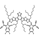 What are Non-Fullerene Acceptors?
Non-fullerene acceptors (NFAs) are organic molecules that, like fullerenes, act as electron acceptors in organic solar cells and other organic electronic devices. However, unlike fullerenes, NFAs lack the hollow cage structure and offer greater flexibility in molecular design, allowing for tunable electronic and optical properties.
Read more...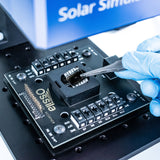 Application of Non-Fullerene Acceptors in Organic Solar Cells
Non-fullerene acceptor (NFA) molecules are currently being used in the active layer of organic solar cells to enhance their efficiency. Organic solar cells, also known as organic photovoltaics (OPVs), consist of several organic components, each playing a distinct role in capturing solar energy.
Read more...An n-type semiconductor is a type of semiconductor where electrons serve as the majority charge carriers, leading to a negative charge transport characteristic. These electron-donating properties make n-type semiconductors suitable for electrical applications, particularly in transistors, LEDs, solar cells and electrodes. The two main types of n-type semiconducting materials are:
Read more...In photovoltaics, researchers are constantly seeking better materials for organic solar cells (OPV). One standout example is Y6, a non-fullerene acceptor (NFA) that is an n-type organic semiconductor. Y6 is commonly paired with a polymer donor in bulk heterojunction solar cells.
Read more... Fine-Tuning A-D-A Small-Molecule Acceptors
Typically, polymer-based organic semiconductors (OSCs) are associated with OPVs. However, small molecules are also showing significant promise in terms of NFAs,2–4 and have similarly tunable properties (such as band-gap width).
Read more... Fullerene vs Non-Fullerene Acceptors for OPVs
Fullerene and non-fullerene acceptors play a pivotal role in organic photovoltaics (OPVs). OPVs are promising candidates for next-generation solar cells due to their lightweight, flexibility, and potential for low-cost production.
Read more...Typically, organic photovoltaics (OPVs) are manufactured in the form of a bulk heterojunction (BHJ) cell, where the active layer consists of a blend of donor and acceptor materials with various interfacial layers and electrodes.
Read more...The majority of organic photovoltaics (OPVs) in research are based upon a binary active-layer mixture (of donor and acceptor materials) in the form of a bulk heterojunction (BHJ).
Read more..."Layer-by-layer" (LbL) processing, also known as "layer-by-layer" deposition, is a technique used for the fabrication of photovoltaic solar cells, in particular organic solar cells. This method involves the sequential addition of ultra-thin layers of materials to build up the device's structure.
Read more... Choosing the Right Spin Coater Chuck
A well-designed and correctly chosen chuck provides stability and balance during the spin coating process. It needs to be able to withstand the rotational forces of a spin coater and also to maintain the substrate firmly in place.
Read more... How to Change Spin Coater Chucks: Video Guide
By following these instructions, you can easily manage the spin coater substrate chucks and achieve better film quality with the polypropylene chucks' recessed design.
Read more... Ossila Contact Angle Goniometer User Manual
The Ossila Contact Angle Goniometer provides a fast, reliable, and easy method to measure the contact angle or surface tension of a droplet.
Read more... Ossila Dip Coater User Manual
Ossila's Dip Coater is a system designed to deposit thin wet films through the controlled immersion and withdrawal of a substrate from a reservoir of solution.
Read more... Ossila Four-Point Probe User Manual
The Ossila Four-Point Probe System is a low-cost solution for rapid and reliable measurement of the sheet resistance, resistivity and conductivity of materials.
Read more... Ossila Glove Box User Manual
Ossila's inert atmosphere Glove Box comes equipped with high accuracy oxygen and humidity sensors, quick purge function and antechamber for quick item transfer.
Read more... Ossila LED Measurement System User Manual
The Ossila LED Measurement System is a low-cost solution for reliable current-voltage-luminance and lifetime measurements of light emitting diodes.
Read more... Ossila Optical Spectrometer User Manual
Ossila's USB powered Optical Spectrometer has been designed to simplify the optical characterisation of thin films, solutions, nanocrystals and more.
Read more... Ossila Potentiostat User Manual
Ossila’s Potentiostat is low-cost and easy-to-use system for performing cyclic voltammetry measurements. Cyclic voltammetry is one of the most widely used electrochemical techniques, providing important information about materials.
Read more... Ossila Slot-Die Coater User Manual
The Ossila Slot-Die Coater has been designed for simple operation and easy maintenance. An integrated high-precision Syringe Pump allows for accurate flow rates.
Read more... Ossila Solar Cell I-V Test System User Manual
The Ossila Solar Cell I-V Test System is a low-cost solution for reliable current-voltage characterisation of photovoltaic devices.
Read more... Ossila Spin Coater User Manual
The vacuum-free Ossila Spin Coater is compact and portable to optimise space in the glove box and produce high-quality coatings without substrate warping.
Read more... Ossila Syringe Pump User Manual
Ossila's Syringe Pump has been designed to move volumes of fluids accurately and repeatedly at specified rates. User manual for single and dual models.
Read more... Ossila Source Measure Unit User Manual
Ossila's Source Measure Unit (SMU) can measure a wide range of research devices including photovoltaics, LEDs and OLEDs, transistors, and more.
Read more... Ossila UV Ozone Cleaner User Manual
Ossila's UV Ozone Cleaner is designed to provide a simple, inexpensive, and efficient method of obtaining ultra-clean surfaces free of organic contaminants.
Read more...The latest software and drivers including our cyclic voltammetry software for the Ossila Potentiostat and more.
Read more... Potentiostat Software Guide
A video guide to using the Ossila Potentiostat software for your cyclic voltammetry experiments.
Read more...View More
Sorry, no pages found. Try removing any filters.