
An Introduction to White Organic Light-Emitting Diodes
White organic light-emitting diodes, known as WOLEDs, emit white light. Emission is typically generated from multiple organic emitter molecules with different emission profiles that collectively cover a broad spectral range. As a result WOLEDs are able to emit light across the full visible spectrum (380 - 780 nm), making them highly versatile for a wide range of lighting and display applications.
The first white organic light-emitting diodes were introduced by Kido and co-workers, marking a significant breakthrough in organic electronics. They developed two types of WOLED device:
- Single light-emitting layer (SEL) composed of a polymer (PVK) with several fluorescent dyes with different emission colours.
- Stacked mode with multiple emitting layers with different carrier transport properties and different emission colours.
Both approaches demonstrated the feasibility of generating white light from organic materials. The researchers were able to produce devices with luminance/brightness of up to 4100 cd/m2. This achievement highlighted the potential of WOLEDs for practical applications in energy-efficient lighting and next-generation display technologies.
WOLED Materials

The materials found in white organic light-emitting diodes are also found in other types of OLED device. The emitting layer(s) contain host molecules and dopant emitting molecules just like any other OLED. The difference being for WOLEDs the light emission must span the visible spectrum in order to produce white light. The dopant material in WOLEDs may be fluorescent, phosphorescent or a combination of the two, referred to as hybrid WOLEDs. Molecules that can undergo thermally activated delayed fluorescence (TADF) also feature in WOLED devices, in order to access more efficient devices that can harness all generated excitons.
Dopant Materials for White Organic Light-Emitting Diodes
Suitable dopant materials for white organic light-emitting diodes encompass a huge range of organic molecules and can emit light via three radiative processes, including:
- Fluorescence
- Phosphorescence
- Thermally activated delayed fluorescence (TADF)
The advantage of phosphorescent over traditional fluorescent molecules is the opportunity to access 100% of the recombined excitons as triplet states excitons can be harvested. However blue phosphorescent molecules suffer from instability and short lifetimes. By combining stable blue fluorescent molecules with phosphorescent green, red, yellow or orange emitters, WOLEDs with high efficiency, stable color and long lifetime can be accessed. The fluorescent blue emitter can undergo triplet-triplet Dexter energy transfer (DET) with surrounding phosphorescent molecules. This means that triplet state excitons can radiatively decay.
Hybrid WOLEDs are common throughout literature where there examples of different combinations of fluorescent and phosphorescent materials including:
Blue fluorophores with low triplet states
Most blue fluorescent molecules used as dopants for highly efficient blue OLEDs exhibit low triplet states. This is due to a combination of electronic, photophysical, and molecular factors related to their emission properties and energy levels. WOLED devices that contain low triplet state blue fluorophores are shown in the table below.
| Device Structure | Blue Fluorophore | Host | Phosphorescent Counterpart(s) | Color | Host | EQE / % | Power Efficiency / lm/W | Luminescence / cd/m2 | CRI |
|---|---|---|---|---|---|---|---|---|---|
| Stacked | BCzVBi | CBP |
PQIr |
Green Red |
CBP | 18.4 | 23.8 | 500 | 85* |
| Stacked | DSA-ph | ADN or MADN | Ir(Cz-CF3) | Orange | CBP | 6.34 | 5.39 | 1000 | 60 |
| Stacked | DSA-ph | Bepp2 |
Ir(ppy)2(acac) Ir(MDQ)2(acac) |
Green Red |
TCTA | 15.2 | 31.1 | 1000 | 74 |
The exciton formation regions occur where electron-hole recombination is most efficient in the white organic light-emitting diodes device. In the device containing BCzVBi as the blue fluorophore, the exciton formation regions were at the interface between the carrier transport layers (ETL and HTL) and their adjacent blue emitting layers (EMLs). The blue EMLs sandwiched a red-green EML with spacer layers between the different colored emitting layers. The spacer layers confined singlet excitons to the blue EML for fluorescent emission. At the same time, triplet excitons could diffuse across the blue EMLs and spacer layers to the red-green phosphorescent emitting layer. This mechanism helps enhance the internal quantum efficiency as both triplet and singlet excitons can be harnessed.
Non-radiative decay can occur when fluorophores have a T1 state that is lower in energy than the T1 state of the phophor. This is because the T1 of the phosphor can undergo Dexter energy transfer to the T1 of the fluorophore where radiative decay is not possible. Due to the large singlet-triplet energy gap in blue fluorescent molecules the excitons in the triplet state can not populate the singlet state. This leads to inefficiencies via non-radiative decay pathways.

Blue fluorophores with high triplet states
Blue fluorophores with high triplet states are the most desirable for hybrid devices when considering triplet harvesting. The high triplet state fluorophores means Dexter energy transfer is directed from the fluorophore to the phosphor where radiative decay can occur. This contributes to high internal quantum efficiencies which contributes to overall device efficiency. One example of a blue fluorophore with a high triplet energy is Bepp2 which has a triplet state as high as 2.6 eV. Some examples of it's use in hybrid WOLEDs are shown in the table below:
| Device Structure | Blue Fluorophore | Phosphorescent Counterpart(s) | Color | Host | EQE / % | Power Efficiency / lm/W | Luminescence / cd/m2 |
|---|---|---|---|---|---|---|---|
| Stacked (Tandem OLED) | Bepp2 |
Ir(MDQ)2(acac) Ir(ppy)2(acac) |
Red Green |
TCTA Bepp2 |
11.9 | 23 | 1000 |
| SEL | Bepp2 |
Ir(PPQ)2(acac) Ir(ppy)2(acac) |
Red Green |
Bepp2 | 30.3 | 1000 |
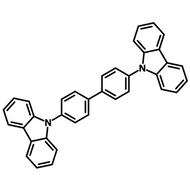
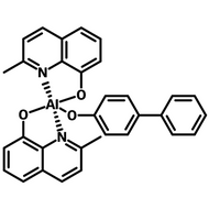
Chemical Structures of WOLED Organic Molecules


The two devices mentioned in the table use Bepp2 as the blue fluorophore and red-green phosphorescent codopants. The key difference between the two devices is the structure, which is discussed further in the next section. One has stacked emitting layers and they other has a single emitting layer. This comparison shows that the single emitting layer device has a better power efficiency at 1000 cd/m2. However, the device does not have stable white emission leading to complicated emission processes. The stacked emission layers offers advantages of better control over the recombination and emission proccesses.
All phosphorescent white organic light-emitting diodes
As molecular design principles have developed, phosphorescent molecules are becoming more stable. This is also supported by the enhancement of various layer device architectures and exciplex hosts to support the dopant materials. As a result there are examples of highly efficient all phosphorescent WOLED devices:
| Device Structure | Phosphors | Color | Host | EQE / % | Power Efficiency / lm/W | Luminescence / cd/m2 |
|---|---|---|---|---|---|---|
| Stacked | FIrpic | Blue | TCTA | ~20 | 40 | 1000 |
|
Ir(2-phq)2(acac) |
Green Red |
TCTA | ||||
| FIrpic | Blue | DCzPPy | ||||
| Stacked | FIrpic | Blue | mCP:B3PYMPM exciplex | 52.6 | 52 | 1000 |
|
Ir(ppy)2(tmd) Ir(mphmq)2(acac)(tmd) |
Green Red |
TCTA:B3PYMPM exciplex |
The first device described in the table above exhibits a triple emitting layer structure. A codoped red and green layer is sandwiched between two blue emitting layers. Through the tailoring of doping concentration and layer thicknesses the energy transfer between dopant and host molecules has been optimised. The second device has a tandem stacked WOLED device structure and has highlighted the importance of horizontally oriented transition dipoles of the phosphorescent dopant molecules.
Host Materials for White Organic Light-Emitting Diodes
Host materials in WOLEDs hold the responsibility of providing a stable environment for the emitting molecules and attracting balanced charge carriers for recombination.
Unipolar vs Bipolar Hosts
Hosts can either be unipolar or bipolar, depending on how it interacts with charge carriers. Unipolar hosts transport either holes or electrons where as bipolar hosts transport both holes and electrons. This property influences where in the device the electron-hole recombination zone is as a bipolar host is more likely to be the area of the device where exciton formation is most efficient. A bipolar host means exciton formation is likely to happen within the emitting layer or layers and contributes to enhancing device efficiency. An example bipolar host is a combination of TCTA (hole transporting) and Bepp2 (electron transporting).
Controlling the exciton formation region is particularly important for multiple stacked emission layer devices. It is important triplet excitons do not become trapped in emissive layers. Trapping can result in non-radiative decay if in a layer with fluorescent molecules. It can also result in triplet excitons not reaching a phosphorescent emitting layer. This can impact color rendering index (CRI), Commission Internationale de L’Eclairage (CIE) coordinates as well as device efficiencies.
In order to promote charge balance, n-type hosts with high triplet state energy levels are often used to remove the barrier of electron injection. This contributes to the lowering of the driving voltages of the WOLED device. However, these molecules are difficult to design. Exciplex hosts offer a simpler alternative to achieving high power efficiencies as they support ambipolar carrier transport and easy carrier injection. This enables high rates of recombination with relatively low turn-on voltages.
Exciplex Materials for White Organic Light-Emitting Diodes
TADF Exciplex Emission
Exciplex complexes enable triplet exciton harvesting through the interaction of electronic donor and acceptor molecules. This property is highly advantageous for improving the efficiency of WOLED hosts and dopants. An example exciplex system is the electron transporting molecule 3P-T2T as the acceptor and the hole transporting molecule TCTA as the donor. There is a large difference between the energy levels of the two molecules. Therefore the interface between the two materials sees an accumulation of charge carriers which increases recombination efficiencies. As a result S1 and T1 exciplex excitons form and the weak donor-acceptor coupling results in a very small singlet-triplet energy ΔEST. This facilitates efficient thermally activated reverse intersystem crossing (RISC) and as a result delayed fluorescence (TADF).
TADF exciplex OLED technology has been adopted by WOLED researchers to the point where all-exciplex-based WOLEDs have been produced. Via a tandem WOLED structure, blue and yellow exciplex systems are combined to emit white light:
| Device Structure | Exciplex D:A | Color | EQE / % | Power Efficiency / lm/W | Luminescence / cd/m2 |
|---|---|---|---|---|---|
| Stacked | mCP:PO-T2T | Blue | 11.6 | 15.8 | 100 |
| DTAF:PO-T2T | Yellow |

Exciplex Hosts
For single emission layer systems host materials are required to efficiently transfer charge to multiple dopant molecules with different energy profiles. An exciplex host has more flexibility in matching the different dopant molecule energy levels through the donor and acceptor selection. Both high-lying and low-lying triplet energy levels can be present in order to access different emission processes. An exciplex with a large triplet energy gap between the donor and the acceptor limits donor–acceptor triplet coupling which can lower the exciplex energy levels. Therefore exciplex hosts can have two triplet states, suiting the different coloured emitters.
White Organic Light-Emitting Diodes Structure
White organic light-emitting diodes have two key structures; single emission layer (SEL) and multiple stacked emission layers. Both have strengths and weaknesses due to their architectures with multiple stacked emission layers being the more explored device structure.

To maximise the amount of photons emitted out of the WOLED the light emitting layer (EML) should be located in at the antinode positions. It is at these points where the electromagnetic waves generated by the emitter molecules are constructively interfered. Therefore the thickness of each layer within the device influences overall device efficiency.
Single Emission Layer White Organic Light-Emitting Diodes
A single emission layer white organic light-emitting diode has just one light emitting layer. SEL WOLEDs typically also include charge transport layers and sometimes charge blocking or injecting layers. The simple device structure is attractive as it sees a reduction in fabrication processes and therefore a reduction in manufacturing costs.
Strategies for multicolor coelectroluminescence in a single emission layer:
- Exciton recombination regulation by doping host with multiple R/G/B guests - energy transfer processes like FRET and DET can be controlled through the careful selection of host and dopant molecules.
- Multicolor emission from a single luminescent dopant material - For triphenylamine derivatives, thermally activated rotation in the molecular structure leads to the enhancement of π–π stacking and electronic coupling. This results in a redshift in some molecules.
In SEL WOLED devices the management of carrier transport and exciton recombination is essential. Within SEL WOLEDs colourful emitters are supported by host molecules. Compatibility between the host and guest emitter molecules plays a huge role in device efficiency. Host molecules often have bipolar characteristics to support the movement of both electrons and holes. Such bipolarity enhances charge balance and creates broader recombination regions. As a result device efficiency and color stability is improved.
The benefits of single emissive layers formed of organic molecules is that vacuum thermal evaporation and spin coating thin film application processes can be used (partly replacing thermal vacuum evaporation).
The drawbacks of SEL WOLEDs are that even with the most simple structures, four organic layers are needed. Due to the risks of self quenching, dopant concentrations are often very low (0.1%) making the control and reproduction of coevaporation procedures difficult.
Stacked White Organic Light-Emitting Diodes
Multiple stacked emitting layer white organic light-emitting diodes have much more complicated structures. They typically include at least two emitting layers that are separated, especially if there operate via different luminescence processes (fluorescent or phosphorescent). To avoid charge trapping and non-radiative decay, interlayers or charge generating layers are also used within the device structure. They help to prevent inefficiencies by directing appropriate charge carriers and excitons to the desired location for recombination or emission.
As well as this the device thickness (between electrodes) and resulting impact on antinode positions must also be carefully considered. Devices with multiple EMLs with different emission wavelengths are placed in different positions for a given total device thickness:
- For a tandem WOLED device, a charge generation layer (CGL), splitting the two WOLED sections, forms two separate recombination zones. Therefore the EMLs can easily be placed in their respective antinode positions.
- For a stacked device that doesn't have a tandem structure, there is just one recombination zone that must satisfy the antinode position of different EMLs. Mismatch of recombination zone and antinode position for any EML can lead to reduced efficiency. Therefore the device thickness must be modified so that the location of the antinode of each EML within the total multiple EML thickness.

Charge Generation Layer (CGL)
The charge generation layer (CGL) is used to enable efficient charge injection and separation in multi-stack or tandem WOLEDs. It generates and injects electrons and holes into adjacent transport layers, allowing multiple emissive layers to operate simultaneously. This improves overall brightness, external quantum efficiency (EQE), and power efficiency by producing more light per unit current. The CGL also enhances device lifetime by distributing the electrical load and reducing degradation, particularly in sensitive emitters like blue. Additionally, it ensures balanced charge injection, preventing energy losses and exciton quenching, making it a key element in high-performance OLED designs.
Interlayers
Interlayers are used in stacked WOLED devices between the emitting layers to control exciton and charge carrier movement. They help to prevent unwanted FRET from fluorescent emitters to phosphorescent emitters and DET the opposite way. Bipolar interlayer materials manage charge carrier balance across the device, helping promote efficient recombination and controlling the recombination zone. This contributes to the increased stability observed in stacked WOLED devices.
Example interlayer materials


Challenges Faced by White Organic Light-Emitting Diodes
Whilst there has been a huge amount of progress in the efficiency and stability of white organic light-emitting diodes since they were first reported in the 90's, they face several challenges. These challenges are current issues and include:
- Complicated Doping: High-efficiency white OLEDs rely on precise host–guest doping processes to balance red, green, and blue emitters for optimal light output. Achieving the correct mixing ratio is challenging and requires iterative design experiments that are both time and energy intensive. Manufacturing often depends on costly vacuum thermal evaporation (VTE) equipment, further driving up production costs.
- Operational Lifetime: Ensuring long operational lifetimes while maintaining stable colour accuracy remains difficult due to material degradation, particularly in blue emitters, which degrade faster than their red and green counterparts. This leads to efficiency losses and colour shifts over time.
- Thermal Management: Thermal management is another issue, as heat generation within the OLED stack can reduce performance and accelerate degradation. Optimising charge carrier balance and minimising energy losses between layers are crucial but complicated tasks, requiring precise control of material interfaces and electrical properties.
- Poor Extraction Efficiency: Occurs when light generated within the emissive layers is trapped by internal reflections, waveguiding effects, or reabsorption within the device stack. Overcoming this challenge involves a combination of material optimisation, device structure improvement, and advanced fabrication methods.
These combined challenges make white organic light-emitting diode development highly intricate, requiring innovation in materials, device architecture, and fabrication techniques to achieve commercially viable, long-lasting, and efficient displays or lighting solutions.
Outlook for WWhite Organic Light-Emitting Diodes
To improve white OLED efficiency, optimising light-extraction methods and internal quantum efficiency (IQE) is critical. While high IQE is possible, much light is lost to internal reflections and waveguiding effects. Key strategies include enhancing the optoelectronic properties of emitter molecules while ensuring long-term operational stability. Addressing their interaction with host materials and processing conditions is vital to prevent degradation, especially in blue emitters.
Strategies for increasing the internal quantum efficiency include:
- Crystal structure regulation improves charge transport and exciton confinement by optimising molecular arrangements and reducing defects that cause non-radiative losses.
- Defect passivation minimises charge trapping and exciton quenching by treating or passivating imperfections within active layers, enhancing both efficiency and stability.
- Interface engineering ensures proper energy-level alignment and charge carrier balance at layer junctions, preventing exciton leakage and improving overall light emission.
Future improvements in external quantum efficiency (EQE) will involve light management techniques like micro-lens arrays, scattering layers, and photonic crystals to extract trapped light. Advanced electrodes, such as flexible or transparent ones, may further boost light transmission. By integrating these strategies with material and design innovations, WOLEDs are expected to achieve higher efficiency, longer lifespans, and increased commercial viability in lighting and displays.
Learn More
 Electroluminescence
Electroluminescence (EL) is the generation of light through the radiative recombination of holes and electrons which have been injected into the material from cathode and anode contacts. The charge carriers are injected into the material due to an applied bias over the cathode and anode. These cathode and anodes are orientated opposite each other.
Read more... TADF Exciplex OLED Technology
A thermally activated delayed fluorescence (TADF) exciplex is an excited-state species that can exhibit thermally activated delayed fluorescence or transfer its energy to a lower-energy emitter. TADF exciplex is formed between electron-donating and electron-accepting molecules by intermolecular charge transfer.
Read more...
References
- Hybrid white OLEDs with fluorophors and phosphors, Chen, J. et al., Materials Today (2014)
- Single‐layer white light‐emitting organic electroluminescent devices based on..., Kido, J. et al., Applied Physics Letters (1995)
- Multilayer White Light-Emitting Organic Electroluminescent Device, Kido, J. et al., Science (1995)
- Highly efficient single-stack hybrid cool white OLED utilizing..., Kim, G. W. et al., Scientific Reports (2018)
- Efficient hybrid white organic light-emitting diodes with extremely..., Liu, B. et al., Sci Rep (2014)
Contributors
Written by
Application Scientist
Diagrams by
Graphic Designer