
Guide to Making Efficient Air-Processed Perovskite Devices
This video provides a guide to making efficient air-processed perovskite devices.
This guide provides information on how to:
- Clean substrates
- Prepare and deposit a PEDOT:PSS hole transport layer (AI 4083 PEDOT:PSS is used in this video)
- Deposit our perovskite precursor ink I101 in air
- Anneal and wipe the perovskite layer
- Spin cast a PC70BM electron-transport layer
- Prepare substrates for a thermally-evaporated top contact
- Encapsulate the devices with encapsulation coverslips and encapsulation epoxy and measure
The structure of the finished device is:
ITO / PEDOT:PSS / CH3NH3PbI3-xClx / PC70BM / Ca / Al
Please note that humidity plays a key factor in the quality of the finished devices; when applying the perovskite layer in air it is essential that humidity is no higher than 40% rh. We have produced a video to demonstrate the effects of high humidity on the perovskite films which you may find valuable.
Following this fabrication routine and using our perovskite ink I101, we have reached a peak power conversion efficiency of 11.7%. We expect to see our customers match and exceed this efficiency with further experimentation, and have therefore created this video to help you kick-start your research programme and immediately create high performance perovskite solar cells.
Additional Information
For more information:
- Read the Full Perovskite Solar Cells Fabrication Guide
- See our perovskite precursor ink I101 product page
- View our full list of perovskite inks
- Contact our technical staff.
Video Transcript:
In this video we will demonstrate the fabrication of perovskite photovoltaic devices having an efficiency of up to 11% by using the Ossila precursor ink.
1. PEDOT:PSS solution preparation
The fabrication of perovskite photovoltaic devices starts by filtering the AI 4083 PEDOT:PSS solution using PVDF filter and a syringe. We find that approximately 1 ml of ink is needed to produce 20 devices. After use, the AI 4083 PEDOT:PSS solution should be returned to the fridge for storage. The filtered AI 4083 PEDOT:PSS solution is allowed to warm to room temperature, ready for deposition on the ITO patterned substrates.
2. Substrate cleaning
To clean your ITO substrates, carefully remove each substrate from its packaging. Be careful to handle the substrates by their sides — don’t touch the ITO coated areas. Load the substrates into the holder one by one — making sure each substrate is securely located.
Prepare a clean glass beaker and boil deionized water containing a little Hellmanex solution. Then place the beaker into an ultrasonic bath filled with boiling deionized water and sonicate for five minutes. The ultrasonic bath causes rapid vibration to occur around the substrates, aiding the removal of particulates. After the five-minute sonication, carefully remove the beaker. Be careful because the beaker will be hot. The substrates should now be dump rinsed in boiling deionized water. It is important to use boiling water to ensure no remaining Helmanex solution is present on the substrates. Perform the dump rinse twice. After the dump rinse make sure you change the deionized water.
The substrates should then be cleaned in Isopropyl alcohol (IPA). Place the substrates in a polypropylene beaker that has a tight-fitting lid. The lid prevents the IPA from evaporating during the sonication. The substrates are again placed into the ultra-sonic bath. Make sure that DI the water is close to boiling point. Sonicate substrates for a further five minutes. Remove the IPA beaker from the bath and carefully remove the lid. The substrates should again be dump rinsed in fresh boiling DI water. Perform the dump rinse twice to remove all the IPA solution from the substrates. Remove the substrates one by one from the holder and place them ITO side upwards on a clean room tissue. Hold the substrates with a pair of tweezers (be careful not to scratch the ITO) and use compression nitrogen to blow away all the water. Carefully lift the substrate and place it on a hot plate and heat to approximately 120 °C.
3. PEDOT:PSS anode preparation
To coat the AI 4083 PEDOT:PSS onto the ITO, place the substrate into a spin coater and spin it at 6000 rpm for 30 seconds. Take 35 μl of AI 4083 PEDOT:PSS solution and dispense it onto the substrate (making sure the micropipette tip is not touching the substrate). Once the substrate has finished spinning, remove it and place it back into the hotplate. Once all the substrates have been coated with AI 4083 PEDOT:PSS, you are ready to spin your perovskite precursor in. It is essential that humidity does not exceed 40% during the application of the perovskite ink. Use a dehumidifier to reduce lab humidity if necessary. The Ossila I101 perovskite precursor ink should be heated for 30–60 minutes at around 70 °C prior to use and held at that temperature during the whole deposition. Transfer the PEDOT:PSS coated substrate from the hotplate and place it onto the Spin Coater and spin it at 3000 rpm. Now dispense 30 μl of ink onto the substrate and begin spinning for 30 seconds. This will produce a bright yellow film. Place the substrate back onto the hotplate at 90 °C.
After all substrates have been coated, use a dry cleanroom swab and wipe the place where preferred contact will go. The swiping removes the perovskite precursor from the surface. Now place the substrates back onto the hotplate and anneal for a further 90-120 minutes to fully convert the mixed halide perovskite precursor. When it’s done, all films should turn from yellow to grey/brown.
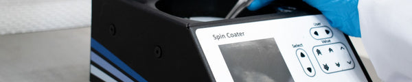
Spin Coater
4. PCBM deposition
Once the perovskite films have been annealed, they can be transported to a nitrogen filled glove box where they will be coated with a PCBM electron-transport layer. Place the substrate in the spin coater (making sure it is secured). Take 20 μl of a filtered PCBM solution and dispense onto the substrate at a spin speed of 1000rpm for 30 seconds. Remove the coated substrate and place on a cleanroom tissue. Take a cotton swab dipped in a Chlorobenzene solution and wipe the PCBM from both edges — making sure not to wipe the active area. After all the substrates have been coated with PCBM, load them into an evaporation mask. Make sure that the substrate is placed correctly with the ITO side facing downwards. Once all the substrates have been labelled and then placed in the evaporation mask, the top of the mask can be secured. Secure the lid with screws in the four corners. This will stop them moving round as they are transferred to the thermal evaporator. Place the evaporation mask into the vacuum chamber. Close the door and secure it before pumping the chamber down.
5. Cathode deposition
A cathode is then evaporated onto the surface of the device. Here you can see the computer system that is used to control the deposition chamber in the evaporation process. After depositing the metal cathode, vent the vacuum chamber and remove the evaporation mask. Take care not to touch the active area of the devices. Open the evaporation mask and lift off the lid. Remove the substrates with the whole mask then place the substrates with the active side faced upwards. Using a pipette, put a drop of UV curable epoxy on the centre of each substrate. Place a glass coverslip on the top of each substrate and press down to allow the epoxy to coat the device. Move the coverslip gently to allow trapped air bubbles to escape. Once all the coverslips have bee placed in position, the substrates are ready to be placed under a UV lamp to be cured for approximately 30 mins. This encapsulates the devices and protects them from moisture and oxygen. The finished devices are now ready to be removed from the glove box.
6. Device testing
Each device is loaded in turn into a test rig and placed under the solar simulator. An aperture mask is used to restrict the active illuminated area. The efficiency of the devices are recorded by measuring a current voltage sweep as they’re illuminated by the solar simulator. We routinely characterize the device open circuit voltage, short circuit current, fill factor and power conversion efficiency. Using the Ossila I101 perovskite precursor ink we routinely obtain power conversion efficiencies greater than 10%.