Reducing Graphene Oxide to Graphene Using Environmentally Safe Materials

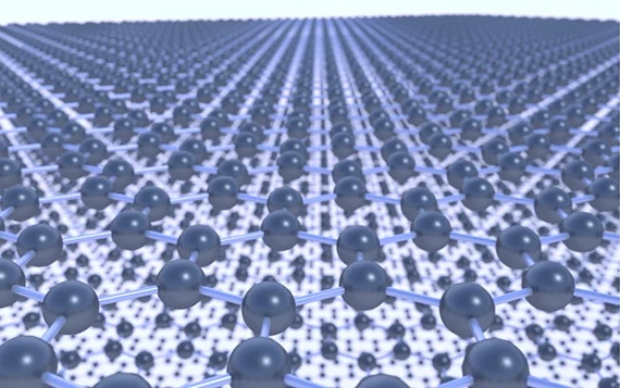
Graphene [1,2] has many potential electronic, optoelectronic and biological uses [3]. However, graphene itself is non-soluble, and this makes it very difficult to deposit from solution (other than from non-stable suspensions). On the other hand, the graphene material, graphene oxide, is highly soluble and very easy to deposit from inks and solutions [4], but at the same time is also insulating and has very few electronic properties of interest.

The conversion of graphene oxide back to graphene is therefore of huge interest to both the scientific and industrial community. At the moment, this process is most typically done with extremely toxic and environmentally hazardous chemicals (such as hydrazine and Lawesson's reagent).
The development of a technique to deposit a uniform, even coating of graphene oxide onto a substrate and convert it to graphene using only environmentally-safe chemicals would facilitate both R&D and industrial exploitation of the mechanical, optical and electrical properties of graphene.
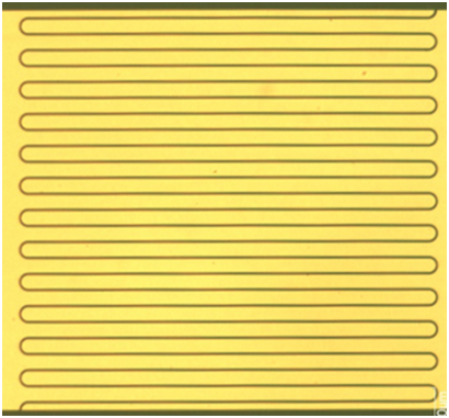
Ossila produce a range of components and data sheets that can enable researchers to quickly and easily undertake this process, whilst making use of our existing infrastructure such as:
- Prefabricated test chips
- Ossila Spin Coater
- Probe Station (discontinued)
- Test & measurement equipment, such as the High Density FET Test Boards.
A thorough literature review suggested that by using a naturally derived reducing agent, namely Vitamin C (L-ascorbic acid) [5,6], it is possible to reduce graphene oxide flakes (deposited onto pre-fabricated test chips from an aqueous dispersion) via spin coating. The results presented below are an adaption of the original work first reported by Zhang et al. in their 2010 paper [5].
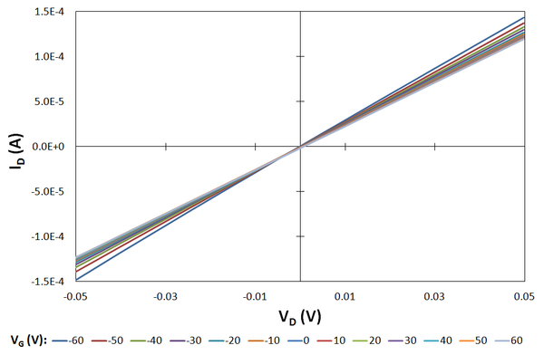
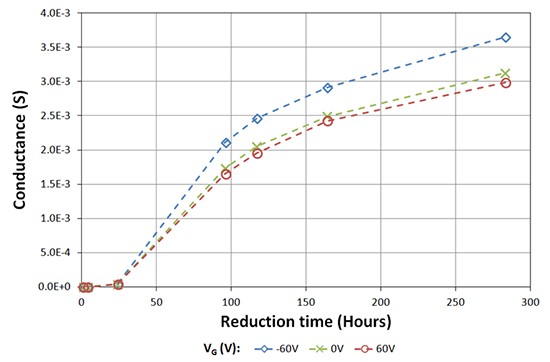
The technique involves the submersion of the pre-fabricated test-chips in a solution of vitamin C in water at room temperature for several days. Optimization on the process time, temperature and concentration is currently ongoing, but initial results are highly promising and, in only a few days work, we were able to produce figures of merit close to those reported in the literature [5]. The rapid speed of progress is largely due to the use of the existing test chip infrastructure, which not only allows for fast electrical measurement but also for single-layer flakes of graphene (oxide) to be located under an optical microscope. This is due to the 300 nm thick silicon dioxide dielectric layer, which is crucial because this specific thickness provides suitable interference to enable the monolayer to be visible on the surface.


If you have any queries or would like more information on our graphene studies please contact us.
Graphene Materials

Learn More
 What is Graphene Oxide?
Graphene oxide (GO) is a two-dimensional material with oxygen-functionalized surfaces, derived from graphite.
Read more... Graphene vs Graphite
Graphene is a single layer of carbon atoms arranged in a hexagonal pattern, like a sheet of paper. Graphite, on the other hand, is made up of many layers of graphene stacked on top of each other, like a stack of paper.
Read more...References
- [1] Nobel Lecture: Graphene: Materials in the Flatland. K.S. Novoselov, Rev. Mod. Phys., 83(3), 837–849 (2011)
- [2] The rise of graphene. A.K. Geim & K.S. Novoselov, 6(3), 183–191 (2007)
- [3] A roadmap for graphene. K.S. Novoselov et al., Nature, 490(7419), 192–200 (2012)