OLED Layers: Substrate (Pixelated Anode) Overview

The pixelated anode substrates come with eight ITO fingers which define the pixels plus an additional cathode bus-bar. The active area deposition mask can be used to evaporate materials onto just the active areas while the cathode mask provides a common connection. The active area is defined by the overlap between the ITO fingers and the cathode with dimensions of 6 mm x 2 mm to produce a total pixel area of 12 mm2.

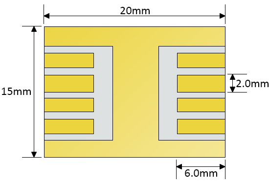
At the core of this system are the pre-patterned ITO-covered glass substrates which are specially manufactured in a commercial LCD fabrication plant. By using high quality ITO from the flat panel display industry we ensure that our substrates are not only capable of high performance but also of high consistency. We use a standardised substrate size of 20 mm x 15 mm and provide a suite of processing equipment and all the consumables required to make finished devices.
Our standard OPV/OLED substrate consists of eight ITO fingers and a cathode connection strip. When combined with our cathode deposition mask, this provides eight pixels of 2 mm by 2 mm as defined by the overlap of the ITO anode (2 mm) and the cathode (2 mm).
The substrates are suitable for variety of deposition techniques including spin-coating, spray-coating, thermal evaporation, printing, doctor blading and Langmuir-Blodgett. They have also been used with a variety of material systems including small molecules, polymers and quantum dots. In short, they provide a versatile platform for a variety of research purposes.
While device fabrication can vary widely depending on the application, we have outlined below a generic fabrication routine for basic polymer-based OPVs or OLEDs. For more detailed instructions please see our fabrication guide and video.
Deposit hole transport layer
Deposit the hole transport layer (for example PEDOT:PSS) and then wipe free the cathode strip afterwards.

Deposit active layer
Deposit the active layer on top of the hole transport layer and again wipe the cathode clean. At this point either an OPV or an OLED can be fabricated simply by using different solutions.

Deposit cathode
Use an Ossila cathode mask to deposit the cathode strips by thermal evaporation or other techniques. These connect the device pixels to the ITO cathode strip which are used to make an electrical connection.

Encapsulate
With Ossila's encapsulation system, devices can be stored for extended durations with minimum degradation in performance. This is ideal for testing devices under ambient conditions. Simply place a drop of Ossila's UV-cured encapsulation epoxy on the device and place the glass coverslip on top before curing in a light box.

Add connection legs
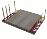
By adding connection legs with a standard 0.1" (2.54 mm) pitch, devices can be inserted into most prototyping boards allowing electrical connection to the eight individual pixels.
Measure
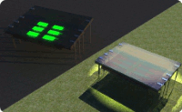
In most cases, device measurements are done through the ITO-covered glass. We also provide aperture masks which fit over the substrates and have eight electrochemically-etched holes above the pixels for more accurate definition of the active area - ideal for OPV measurements with a solar simulator.
Substrates and Fabrication

Learn More
 OLED Fabrication Guide
In this guide, we demonstrate how to make standard OLED devices in a glove box using materials and equipment easily available to any lab. Find out more.
Read more... OLED Testing Guide
This guide gives you an overview of what to consider when characterising an OLED, as well as tips for their measurement.
Read more...