
OLED Fabrication Guide
In this guide, we demonstrate how to make standard organic light-emitting diodes (OLEDs) in a glove box using materials and equipment widely available to any lab. Fabricating OLED devices using Ossila’s pre-patterned ITO substrates is designed to be quick and easy. We've included every detail that we can in this manual so that you can produce efficient devices with as little effort as possible.
For the reference device described here, there are seven basic steps that take you from substrates to devices ready for measurement. Within this guide, you will find detailed information on each of these steps along with any additional information that we have collated which enables better fabrication.
Required consumables, chemicals and equipment
The required consumables, chemicals and equipment to make OLED devices that can be tested using the LED measurement system, are shown in the table below:
| Process chemicals and consumables required | Processing equipment required/used |
|---|---|
|
|
Safety and Operating Conditions
Safety Notice
Please read all relevant Material Safety Data Sheets (MSDS) and create a Risk Assessment for this process before commencing fabrication. In general, care should always be taken when handling the glass substrates as they are relatively thin and can potentially be broken, creating sharp edges.
Sodium hydroxide (NaOH) solutions are used during the cleaning processes, and proper personal protective equipment should be used. Care should also be taken to ensure all personnel are aware of how these solutions should be created and disposed of. Special hazards include the exothermic reaction of sodium hydroxide pellets with water when making stock solutions (NaOH should always be added to water and not the other way around), and also the fact that the NaOH solutions should never be disposed of with solvents.
Operating Conditions and Handling
We recommend fabricating in a class 1000 cleanroom to produce results with as high a consistency as possible. OLEDs are relatively tolerant to dust, but it is insulating and stops function where is lands on the surface leading to black spots in the device. As this is typically a small fraction of the active area it is therefore possible to fabricate outside of a cleanroom so long as some care is taken.
One particular problem is that dust can change the surface-wetting properties where it has landed on the substrate — leading to pinholes and therefore shorting of devices. This is particularly relevant when spin coating of PEDOT:PSS on the ITO which needs to be in pristine condition.
Processing without a glove box is also possible but does cause some issues which need to be considered. Thin films of PEDOT:PSS are hygroscopic and absorb water very easily from the atmosphere, which leads to phase separation of the PEDOT from the PSS which degrades performance rapidly. The active layer can also be degraded by oxygen and water, especially in the presence of light. Processing under low-intensity red light significantly improves the stability of thin films of active layers, but it is still essential to minimize the exposure time. Reactive interface layers such as calcium must also be avoided when processing in air.
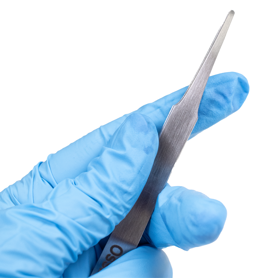
One of the most important factors in a fabrication run is the handling of the substrates. Substrates should generally only be handled with tweezers. Care must be taken to avoid touching the active areas, as this will scratch the films and cause failures due to shorting of the anode and cathode. The diagram below shows the active areas in red which must not be touched by the tweezers as well as the safe handling zone.

It is also essential the substrates should be kept the right way up. Even though a surface may appear physically clean, this is not the same as a surface being chemically clean. Where the active surface has been in contact with other surfaces (even clean surfaces such as cleanroom tissues) this typically leads to device defects. As such, substrates that have been dropped and landed active face down should be discarded to ensure device data is not affected.
For easiest handling of substrates we recommend using 2A-type tweezers with rounded noses such as below.
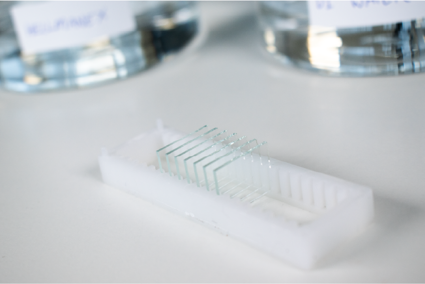
Substrate Cleaning Step
Please note that these substrates are now packaged in clean room paper instead of the protective photoresist coating of older batches.
This sodium hydroxide (NaOH) cleaning routine will help remove any dust and also provide a hydrophilic surface without the need for a plasma or UV clean (note that some materials/solutions particularly close to the wetting envelope may still benefit from a plasma clean).
Ossila has discontinued the use of photoresist to protect the substrates for the following reasons:
- The exact strip routine was dependent upon the power and temperature of the sonic bath, so getting it right was overly time-consuming.
- Many users kept the substrates for a long time (sometimes years) and we found that the photoresist became slightly harder to remove over that timescale.
- If exposed to excessive heat, the photoresist could become plasticized and stick the substrates together.
For any queries that you may have, please contact us for more information.
Cleaning routine
Ossila's pre-patterned device substrates are made from the same ITO-covered glass panels used in the display industry to ensure that the ITO is of extremely high quality and defect-free. To preserve the quality of the ITO surface during shipping and storage it is shipped in clean-room paper. This means that a simple cleaning routine, which can take as little as 20 minutes, can be used to provide a pristine ITO surface without the need for plasma ashing of the substrate.
The first step is to load the substrates into the cleaning rack such that they all have the same orientation. To identify the ITO side simply look at the edge of the substrate at an oblique angle — the ITO should be seen to go all the way to the edge when facing towards the viewer. If you are unsure, you can use a multimeter to measure the resistance across the ITO surface, which should be low due to its conductivity.

For substrates with no photoresist coating:
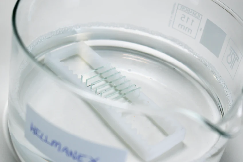
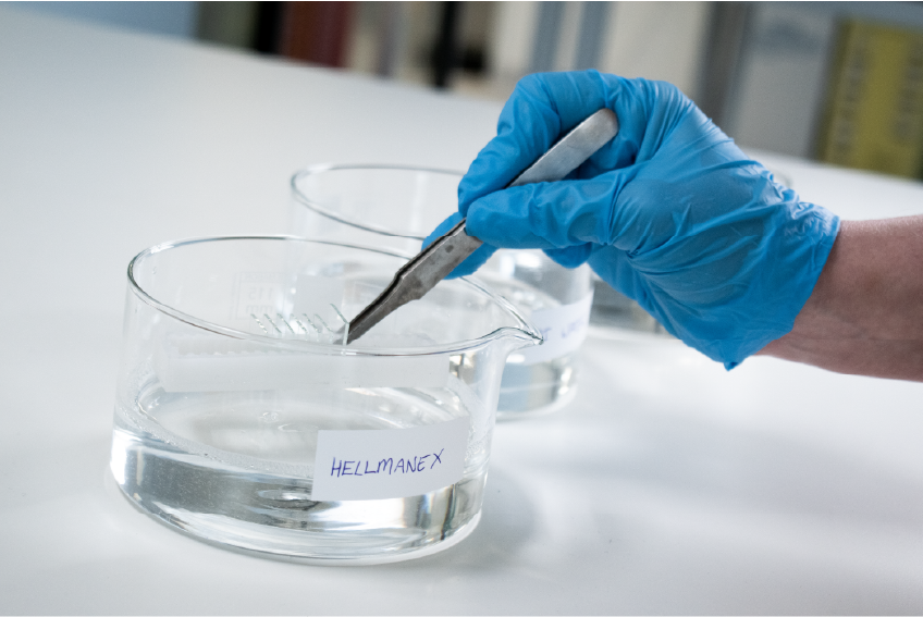
The loaded substrate rack is submerged in a beaker with 1% (by volume) Hellmanex solution in hot (boiling) water. This is to remove the majority of contaminants, such as dirt and dust. The breaker is placed into a sonicator filled with boiling water from a kettle and sonicated for five minutes.
After sonication, the substrates should be thoroughly rinsed with water. This can be done by either: placing them under a running tap, or submersing them in at least two consecutive beakers of water (dump rinses).
The loaded substrate rack is then placed in a beaker of isopropyl alcohol (IPA) and sonicated for 5 minutes, using the same hot water that is remaining in the sonicator. This is to remove any remaining organic residues. Again rinse thoroughly with water as mentioned above.
Finally, to finish cleaning and ensure a hydrophobic substrate surface, the substrates are sonicated in a 10 wt.% solution of sodium hydroxide (NaOH) in water.
Note that extra care must be used when handling hot NaOH solutions, and of course personal protective equipment should always be used.
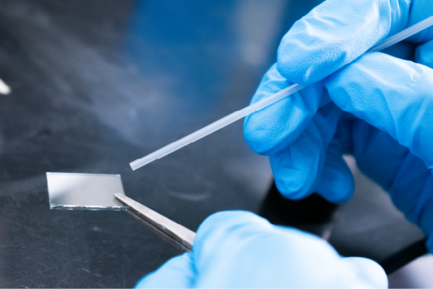
When rinsing, rinse first with hot water and again with cold water. Keep the substrates immersed in water until ready to blow dry in order to avoid contamination by dust.
When blow drying, always hold the substrates down at the edge on the cathode side and blow the nitrogen towards the tweezers so that any dirt on the tweezers does not re-contaminate the active area.
Summary of substrate cleaning:
- Sonicate in 1% (by volume) Hellmanex solution for 5 minutes
- Rinse thoroughly twice in hot water
- Sonicate in IPA for 5 minutes
- Rinse thoroughly twice in water
- Sonicate in 10 wt.% NaOH solution for 5 minutes
- Rinse thoroughly twice, once in hot and once in cold water
- Store immersed in water until required
- N2 blow dry
Note: To prepare a 10% by weight solution, dissolve 100 g of NaOH into 900 g (900 ml) of water to give a total solution mass of 1000 g.
- Sonicate in 10 wt.% NaOH solution
- Rinse thoroughly in water
- Sonicate in fresh 10% NaOH solution
- Rinse thoroughly in water
- Store immersed in water until required
- Blow dry with nitrogen
Applying the Hole Transport Layer
We recommend using PEDOT:PSS as the hole transport layer. The PEDOT:PSS layer performs three functions:
- Planerisation of the ITO surface,
- Matching of the ITO interface energy with the light emitting layer layer
- Acts as a hole only (electron blocking) transport layer.
Getting a high quality PEDOT:PSS film is critical for effective device performance and is often the most difficult part of device fabrication. PEDOT:PSS requires a pristine and hydrophilic surface in order to coat properly, which should have been achieved with the cleaning routine above. It is also critical to ensure that the active areas have not come into contact with any other surfaces as this will affect how well the ITO will spin.
Note: At this point you can use Kapton® Tape (polyimide film with silicone adhesive) to cover the electrode areas, ensuring the exposed area matches the shape of the desired active area.
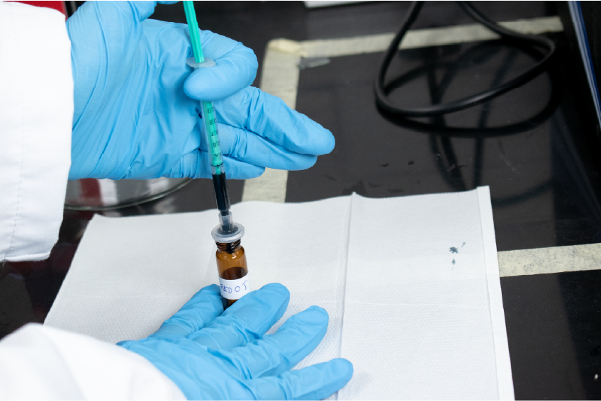
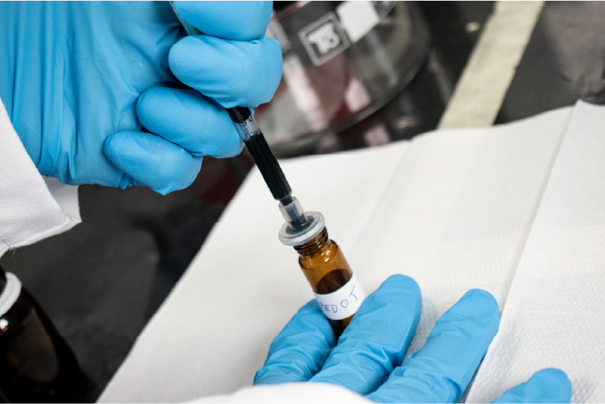
The grade and composition of PEDOT:PSS is also very important. We use PEDOT:PSS AI 4083 which is filtered prior to use through a 0.45 μm PES filter.
Note: It is very important to use a rubber-free syringe as many rubbers are attacked by the acidic nature of the PEDOT:PSS.
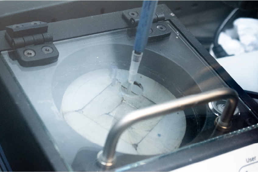
For typical use in OLEDs, we spin coat the PEDOT:PSS at 5000 – 6000 rpm for 30 seconds to produce a film thickness of 30 – 40 nm. To minimize material use this can be done by pipetting 20 to 30 μl into the middle of a spinning substrate. After spinning has completed, visually inspect the PEDOT:PSS films for defects. For best performance discard any substrates with imperfections near the active pixels.
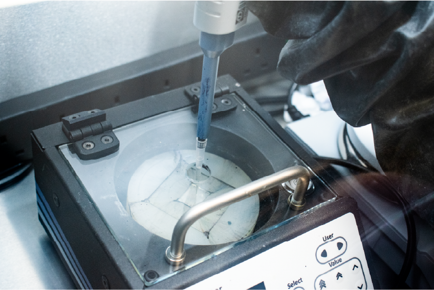
It is useful to number the under-side of the substrate at this point with a permanent marker, for later substrate identification. Then place the substrates either in a box with the lid closed to avoid dust settling on devices, or if kept in air for more than a few minutes place directly on a hotplate.
At this point you can remove the PEDOT:PSS off the ITO fingers around the edge of the substrate but we recommend waiting until you have deposited all of the desired layers.
For best performance, the PEDOT:PSS should be annealed on a hotplate. We have tried making devices with different PEDOT:PSS annealing times from 1 min to 1 hour and temperatures from 75 to 180°C and demonstrated that initial performance is not affected by this regime so long as the devices were stored in a glove box during this time. As such, a quick anneal of 5 min at 150°C is used for our standard processing in order to remove any residual water.
It is critical to minimize the exposure of the PEDOT:PSS thin films to air as performance will rapidly degrade. The films are stable while on a hotplate and also while inside the glove box, however, when exposed to ambient conditions they undergo what is assumed to be a morphological change due to solvent annealing from moisture in the atmosphere and resulting in an insulating PSS rich layer at the surface which significantly degrades performance.
Summary of PEDOT:PSS preparation
- Filter the PEDOT:PSS (0.45 μm PES)
- Spin coat at 5000 rpm for 30 seconds
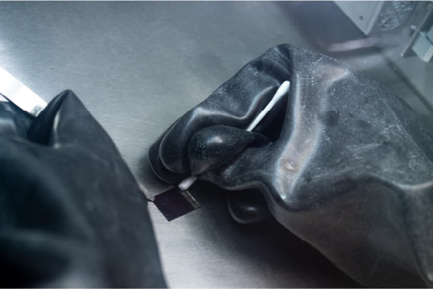
- Wipe the cathode with a cleanroom swab / water
- Bake for 5 mins at 150°C
- If spun outside the glove box store on the hotplate until ready for use
Applying Light Emitting Layer
The light emitting layer can be applied either in air or in a glove box with little difference in performance provided exposure time and light levels are minimized. In general spin coating in a glove box ensures more controlled conditions.
The deposition conditions of the light emitting layer depends on the materials you want to use. The standard reference solutions we typically use are:
OLED reference with typical brightness of 100 cd/m2:
- F8 with F8BT
- Blend ratio of 19:1 (F8:F8BT) in Toluene
- Total concentration of 15 mg/ml
- 0.45 μm PTFE (hydrophobic) filter
- Spun at 2000 rpm (80 nm thickness)
Pipetting 20 μl of the above solution onto a substrate spinning at 2000 rpm should provide a good, even coverage with an approximate desired thickness. The substrate needs to be spun until dry, which is typically only a few seconds — 15 seconds should be ample to achieve this for the above solutions and any other solutions based on toluene, chlorobenzene or chloroform. Solutions based on dichlorobenzene or other high boiling point solvents may need several minutes of spin coating to dry fully.
Following spin coating, the samples can be solvent or thermally annealed if desired. For this OLED reference solution, we recommend thermal annealing at 80 °C for 10 minutes.
Before cathode deposition, the ITO fingers and cathode strip needs to be wiped clean. It would be at this point you would remove the tape if you had used it. Or a cleanroom swab dipped in toluene can be used to remove material from those areas. Make sure the cleanroom swab is not too wet as the solvent will wick across the film and damage the organic layers.
Finally, the substrates need to be placed face down in the evaporation shadow mask with the cathode strip at the wide end of the apertures. This is the only time the substrates should be placed with the active face down.
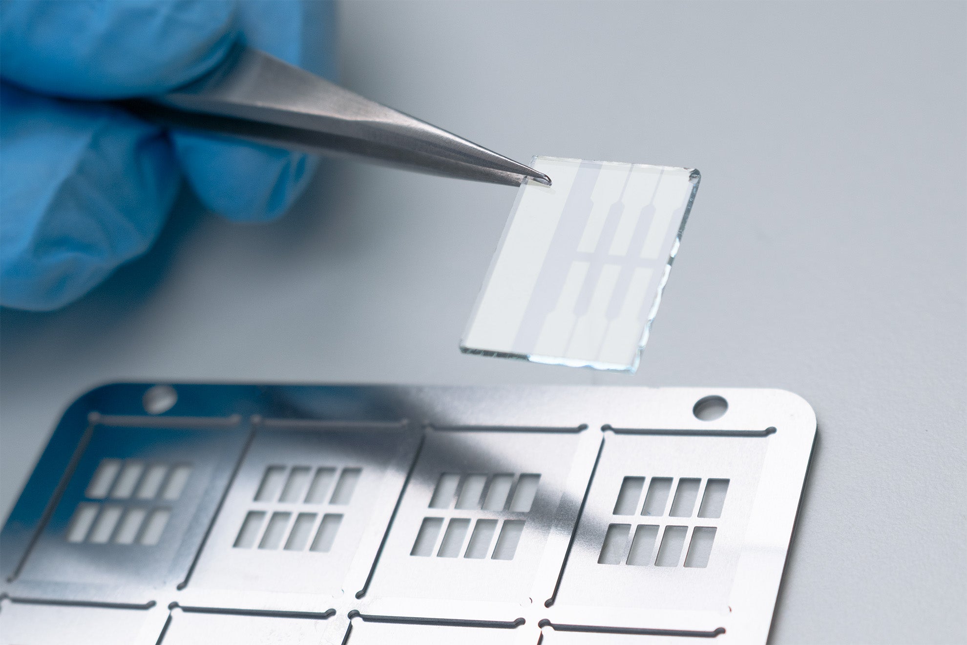
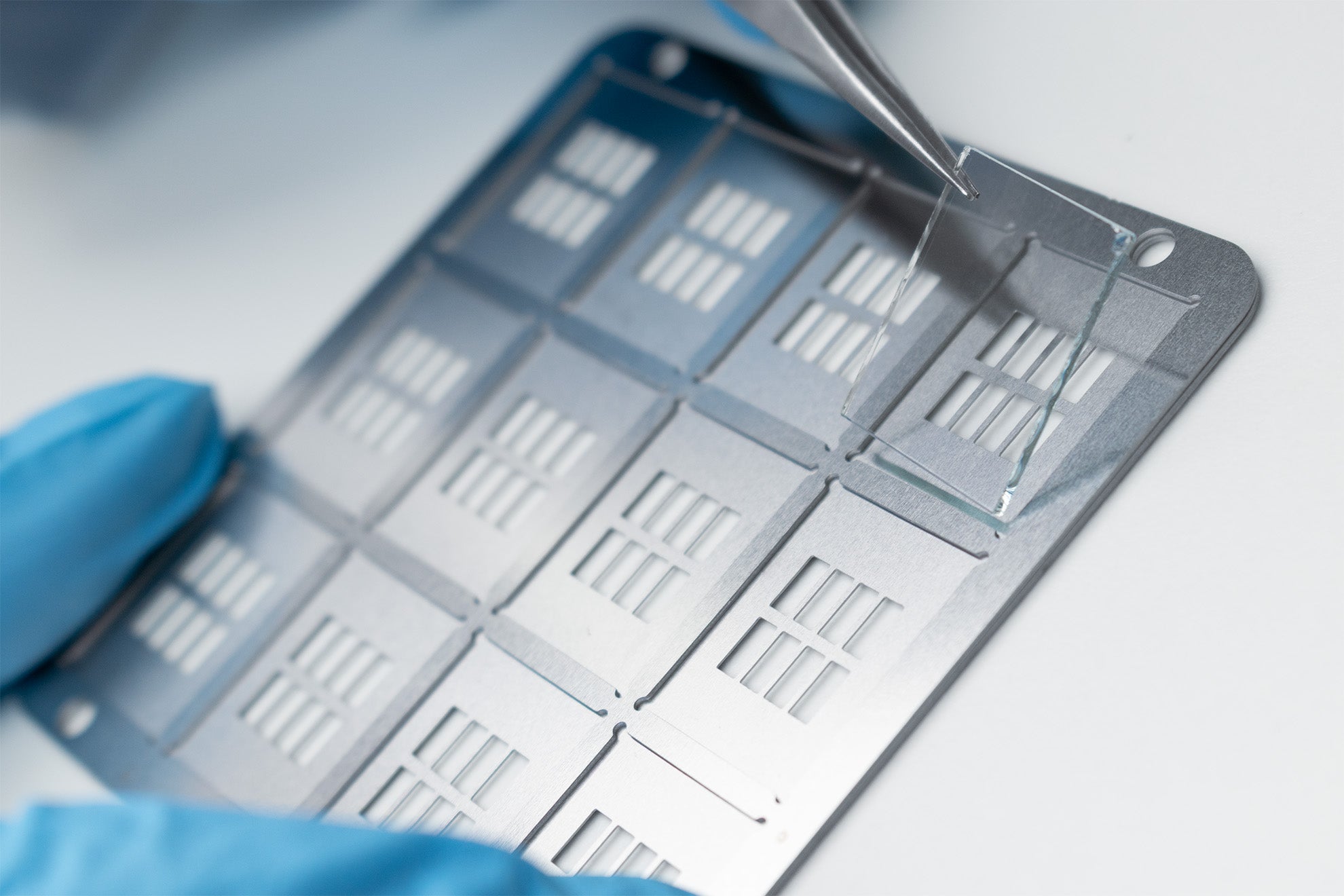
The deposition masks that are compatible with Ossila’s pre-patterned ITO substrates (25 mm x 25 mm or 20 mm x 15 mm) and LED measurement system are shown below:


The diagrams above show just a couple of types of deposition mask that are appropriate for OLED devices. The mask most suited to your work depends on the size and number of pixels that you desire. Please get in touch if you are unsure.
Evaporating the Cathode Layer
For OLED devices the reference cathode is calcium or aluminum. Cathode evaporation is in general the trickiest and most failure prone part of the fabrication process.
The evaporation of aluminum is notoriously difficult as not only is molten aluminum highly reactive but it also tends to wet the sides of the crucible to the extent that it flows over the rim and corrodes the heating element. A good evaporation procedure that minimizes the volume and temperature of the aluminum in the crucible can minimize these problems. As a result, the heating element and crucible can be re-used many times with good reliability (our record is 49 evaporations from one crucible/heater).
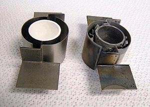
We have used several evaporators with the crucible and heating element dependent upon the power sources and the throw (distance between the crucible and sample). We find that boron nitride crucibles with tantalum heating elements provide good reliability for larger evaporators and tungsten filaments work well for small evaporators.
Typically, we evaporate 100 nm of aluminum at a rate of around 1.5 Å/s, but thinner cathodes (50 nm) have also been used with no decrease in initial performance noted. The deposition rate can also be increased but this also increases the likelihood of the aluminum getting onto the heater and damaging it.
It may take a little practice to get an aluminum evaporation working well, however, once a good procedure is in place it should be possible to get many evaporations per crucible and heater.
Calcium evaporation is relatively trivial as it melts at low temperatures. It can only be used effectively in conjunction with a glove box otherwise degradation occurs. While working OLEDs can be made without calcium, its presence significantly improves performance.
Thermal Annealing Step
After cathode deposition, thermal annealing can be performed if required. Annealing at a temperature of approximately 150 °C for 15 minutes gives optimal performance. Note however, that there is often a discrepancy between the hotplate readout and the actual surface temperature of up to ten degrees, so this is worth calibrating carefully. Also be careful when removing the samples from the hotplate as at this temperature they can melt gloves and cleanroom paper.
Encapsulation Step
Encapsulating the devices protects them against degradation by oxygen and moisture once removed from the glove box. True encapsulation for lifetimes of thousands of hours requires the use of glass welding technology and/or getter layers of calcium. Ossila has developed a quick and effective way of encapsulating devices for lifetimes of several weeks or months under ambient conditions by use of a specialized epoxy.
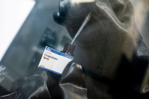
Ossila's UV curable epoxy has been specially selected to provide effective encapsulation while avoiding damaging the polymer or cathode underneath it during the setting process. By using this epoxy to bond a glass coverslip on top of the substrate Ossila’s substrates can be used without degradation over the course of several weeks. Curing is achieved by using a low power UV light of 380 nm over the course of about 30 mins.
Note that if using the epoxy in a glove box then it must be given several days to outgas any absorbed oxygen/water before being applied to sensitive layers such as calcium.
The highest performing devices are produced by encapsulating after annealing has been done. However, encapsulation can also be done before annealing with only a small decrease in performance and allows for measurements to be made outside the glove box at different annealing times and temperatures.
To encapsulate a device, simply use a pipette tip to deposit a single drop of the UV curable epoxy onto the middle of the cathode and then place a coverslip on top of it. Over the course of around 30 seconds the encapsulant will spread out under the coverslip, and after checking for voids, can be placed in a UV light box to set. You can view a video demonstration of this process on the encapsulation epoxy product page.
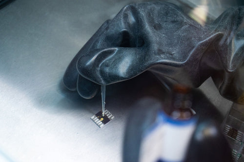
Attaching the Electrical Legs
This video demonstrates how to connect electrical legs to substrates for measurement using zero insertion force (ZIF) sockets.
Attaching connection legs to devices enables easy and repeatable measurements. The connection legs can be attached by placing them on a flat surface (clip side up) and then placing the substrate vertically on the clips before gently pressing down such that they engage. This step can then be repeated for the other side of the substrate. Visually inspect the legs to check their alignment with the ITO as misalignment can cause measurement errors as more than one pixel will be active at once resulting in an artificial doubling of performance. This process can be made easier by first scraping the substrate edges with sandpaper.
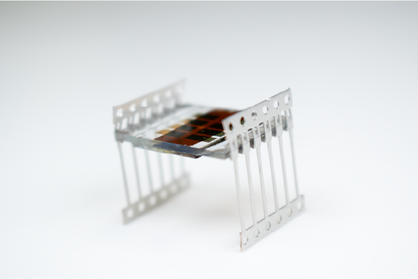
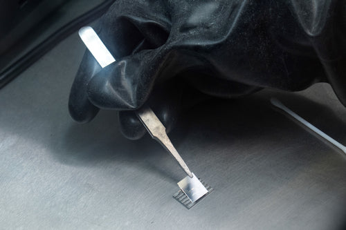
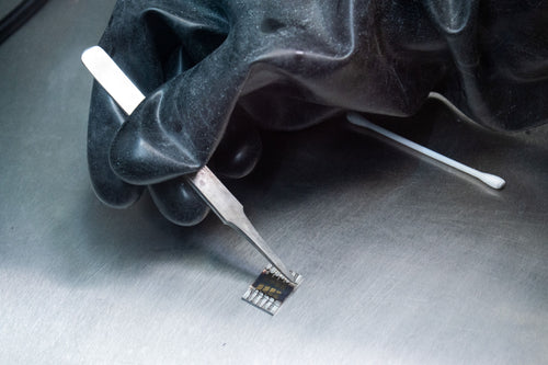
Extra care should be taken when engaging the substrates in the legs and only gentle pressure should be applied as there is the potential to break the substrate.
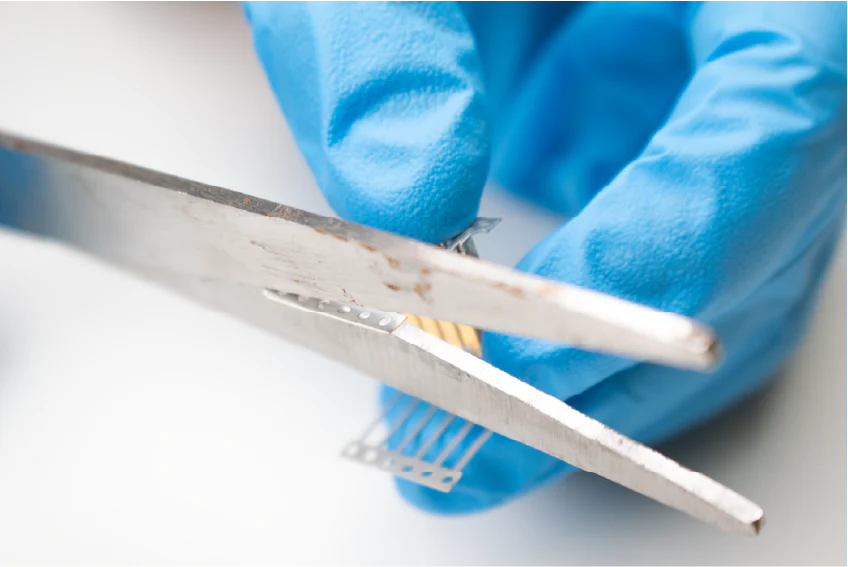
After the legs have been attached, the bottom and top of the legs must then be removed. This can be done with a sturdy pair of scissors while the top can be removed by holding the substrate in one hand with the thumb and fore-finger and gently bending the top until it snaps off. Recheck the alignment of the legs with the ITO as they can be moved slightly during the cutting process.
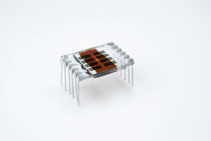
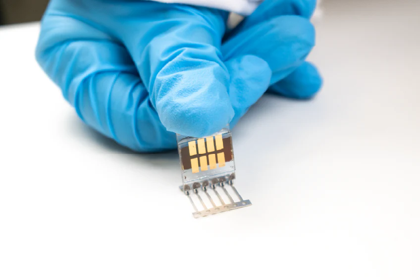
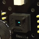
Ossila's ZIF sockets allow easy measurement using a variety of test equipment via the BNC connector. Simply raise the arms on the ZIF socket and place the substrate in. Lower the arms to make electrical connections and then select individual pixels using the micro-switches on the board.
OLED Materials
Learn More
 OLED Testing Guide
This guide gives you an overview of what to consider when characterising an OLED, as well as tips for their measurement.
Read more...The schematics below show the layout of the substrates along with the available deposition shadow masks. The pixelated anode substrates come with six ITO fingers which define the pixels plus an additional cathode bus-bar.
Read more...