How to Make Efficient Perovskite Solar Cells in a Glove Box
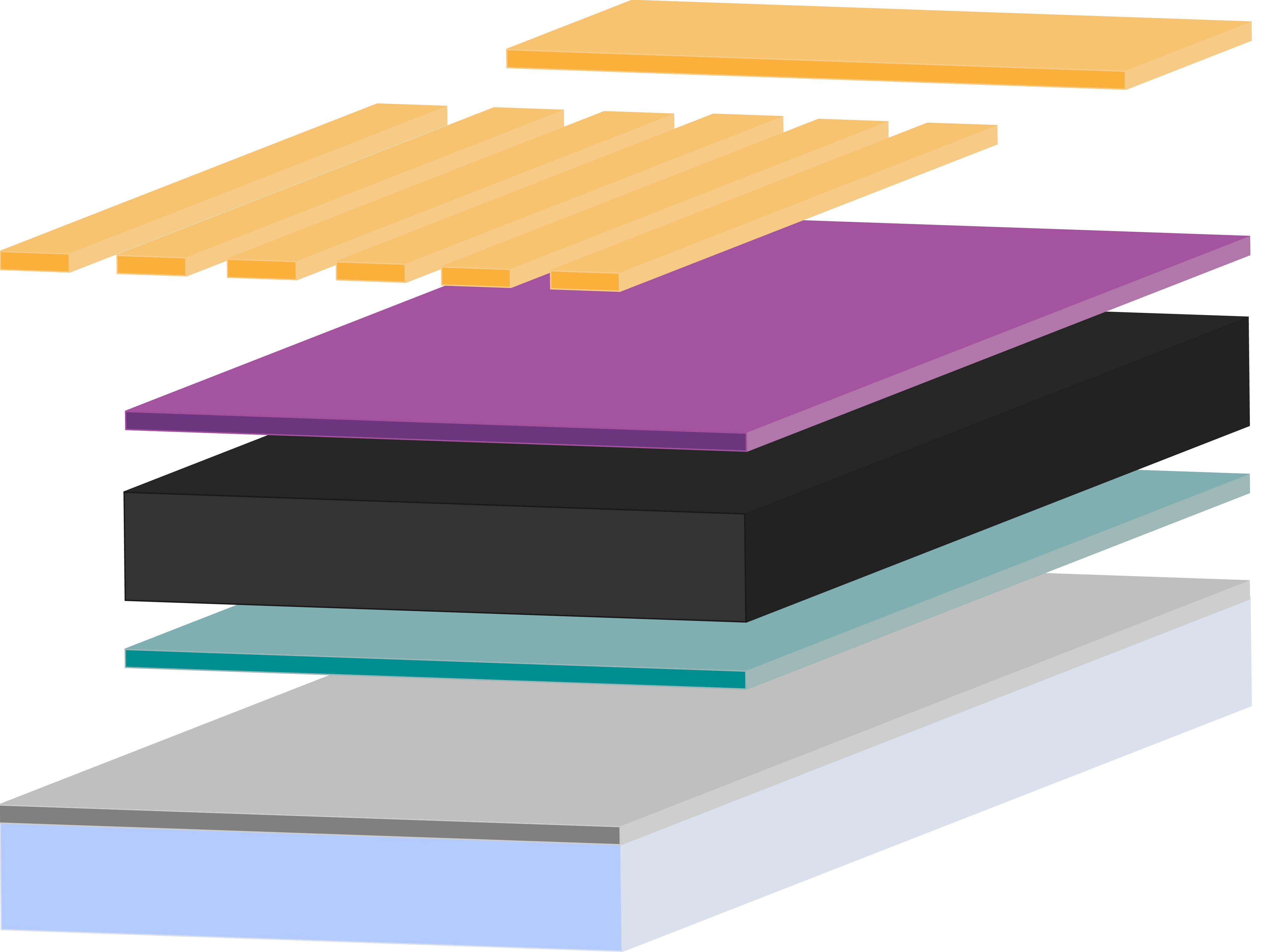
This video details how to make highly efficient perovskite solar cells using the Ossila I301 ink with the following device stack:
ITO-coated glass / SnO2 / I301 / Spiro-OMeTAD / Au
Various other perovksites and transport materials, along with references and examples of their uses, can be found on our "Ultimate Guide to Perovskites" page - but we thought it would be useful to demonstrate an example of how to make a PSC (that can acheive over 19% PCE), from start to finish. We've also tried to include some helpful tips to perfect your technique.
Specifically, this guide details how to:
- Wash and prepare substrates for fabricating devices
- Create SnO2 ETL in air
- Deposit an I301 perovskite layer in the Ossila Glove Box
- Deposit a uniform Spiro-OMeTAD layer in the Ossila Glove Box
- Finish and test devices
Ossila products used in this video:
- UV ozone cleaner
- ITO patterned glass substrates
- I301 perovskite precursor
- Spiro-OMeTAD
- Glove box
- Spin coater
- Measurement aperture mask
- Busbar deposition mask
- Solar cell IV test system
Before starting the device making process, we recommend weighing out all solutions, dopants, and precursors beforehand using a calibrated microbalance. Small variations in the measurements can affect the stoichiometry and, subsequently, the performance of your devices. It’s also a good idea to avoid preparing less than 1 ml of any material, as smaller volumes can introduce inaccuracies and lead to uneven layer deposition or inconsistent results.
The video transcript is contained below:
- Substrate cleaning:
- Rub ITO between (gloved) fingers with Hellmanex then thoroughly rinse with water to remove all trace of hellmanex from the substrates.
- Sonicate for a period of time (we reccommend 10+ minutes) in deionised water/hellmanex combination, then rinse with a lot of boiling DI water.
- Sonicate briefly or dunk rinse in DI water.
- Rinse and sonicate ITO for 15 minutes in isopropyl alcohol (IPA).
- For best device performance, rinse and sonicate for 15 minutes in Acetone and subsequently rinse and sonicate as above in IPA.
- Then, dry substrates using filtered compressed gas and place the ITO into the UV Ozone cleaner and clean for at least 15 minutes.
Mary's comments: When striving for uniformity across a whole substrate, cleaning is a very important step. In particular, the step where you rub the substrate with hellmanex and gloved hands seems to make a big difference, as you can physically remove any dirt/dust before starting the cleaning process.
Mary's comments: Before depositing each new layer, it is a good idea to remove any new dust particles by blowing on the device surface with compressed gas such as N2. This will reduce the amount of defects/comets in your film. Additionally, when spin coating, lower the lid gently if there is a substrate in the chuck, so as not to knock dust particles from the lid down onto the substrate.
- SnO2 ETL deposition:
- Create a 3% dilution of SnO2 nanoparticles in DI water.
- Take substrate straight from UV Ozone to the spin coater and statically spin coat 50μl of SnO2 at 3000rpm for 30s.
- Using a cotton bud and DI water, pattern devices as necessary.
- Anneal for 20-40 mins at 150°C.
Mary's comments: UV Ozone treating substrates before depositing the SnO2 and perovskite layers improves wettability substantially, which will help create homogenous layers, leading to good device performance across the substrate. The effects of "UV-Ozone-ing" your devices last for ~30 minutes, so if your devices are waiting around a lot before deposition (there are always unforeseen dramas to contend with when making devices), it is always a good idea to UV Ozone them again as close to deposition as possible.
- Perovskite deposition (in glove box):
- Transfer the substrates into an inert environment glove box.
- Filter perovksite precursor using a 0.2μl filter.
- Place substrates inside the spin coater and dispense 35 μl of I301 ink all accross the substrate.
- This deposition requires a 2 step spin programme. Firstly, 1000 rpm for 10s, then an secoond step of 3000 rpm for 28s.
- 18 seconds into the second spin step, dispense 100μl of antisolvent to quench the perovskite and leave to spin for a further 15s (the quenching should be done using a slow, continuous stream of solvent over at least 1 second).
- Place substrate back onto the hotplate at 130°C for 10 minutes.
Mary's tip: When depositing perovskite or transport layers within the Ossila Glove Box, it may help to circulate N2 through your system.
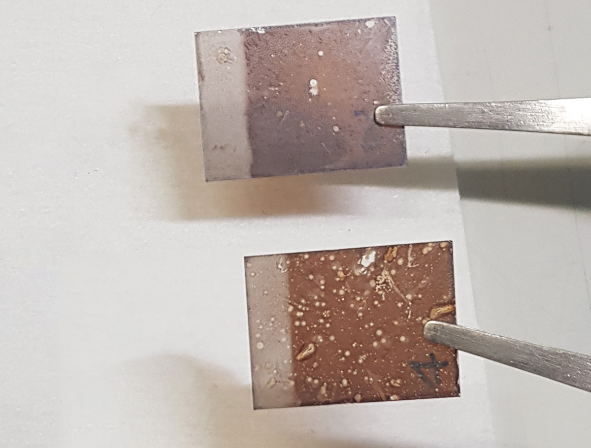
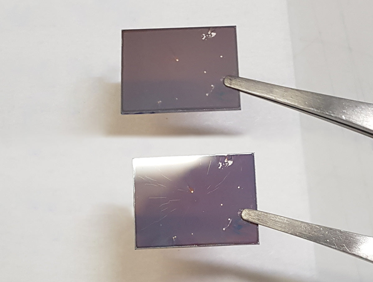
However, it is important to ensure the glove box is as clean as possible before processing perovskite devices on this. Circulating N2 within the glove box may kick up any dust that lies within the system. This can cause a lot of pinholes in the perovskite films, leading to shorts within the devices. If you are finding this to be a problem, it may be best to start a circulation cycle a few minutes before you begin processing. Then wait for ~1minute after the circulation cycle is done before beginning working in the glove box. Repeat this cycle, taking regular breaks to purge the glove box then allow the environment to settle before beginning work again. See below a film made without the glove box purging (left) and a film made while the glove box was purging (right).


- Spiro-OMeTAD deposition (in glove box):
- Prepare the following solutions:
- Spiro-OMeTAD (sublimed) at a concentration of 85-86 mg/ml in chlorobenzene
- Li-TFSI at a concentration of 500 mg/ml in acetonitrile
- TBP at a volumetric percentage of 98%.
- FK209 Co (III) TFSI at a concentration of 300 mg/ml in acetonitrile
- For 1ml of solution, dissolve 85mg of Spiro-OMeTAD (sublimed) in 1ml of chlorobenzene and leave to sit for a couple of hours. (For reference 1ml will coat ~20 [2.0 x 1.5cm] substrates.)
- Add dopants to this solution in this order and dissolve for a full minute after each addition:
20μl Li-TFSI
34μl TBP
11μl of FK209 Co (III) TFSI. - Filter solution using a 0.2μm filter.
- Place perovskite-coated substrate in the spin coater and start spinning at 4000 rpm for 30 seconds.
- During this, dynamically dispense 25 µl of the Spiro-OMeTAD solution onto the substrate to create a uniform layer with minimal pinholes or comets.
- Spiro-OMeTAD oxidation and anode deposition:
- Remove devices from the glove box and store in a dry place away from UV light overnight. This gives the spiro-OMeTAD layer to oxidise fully, improving device performance.
- Using tweezers or a razor, scratch away the perovskite and spiro-OMeTAD layer as before (see 8-pixel patterning guide for more information)
- Using thermal evaporation, deposit at least 75nm layer of gold through the appropriate aperture mask to define an active area for your device (we recommend the use of our 8-pixel busbar maskk for optimal device performance)
- Devices can be measured immediately after being taken out of the glove box, but a performance improvement of up to 3% has been seen if devices are left to rest in air for another 12 hours after gold deposition.
Mary's comments: If the metal contacts of your devices wear away whilst testing, or even to improve charge transport to the testing pins, paint a thin line of conductive paint along the pins of your device. This will encourage charge extraction, especially in pre-patterned ITO devices that rely on heavily on the ITO for charge transport to the pins.
- Testing Devices + Tracking Performance
- Current-Voltage sweeps can be performed on a PSC to measure PCE, VOC, JSC and fill factor. In this video we use an automatic IV tester which cycles through different pixels, sweeps voltage and measures current automatically, and a Newport 92251A-1000 solar simulator. It is very important that this is regularly calibrated to ensure accurate measurement.
- Device area can be defined with a aperture mask of known area, such as our 8-pixel aperture mask. This is your "active area" so it is worth regularly measuring this area with an optical microscope to ensure this value is correct.
- To confirm that device hysteresis is not creating false efficiencies, fixed-power-point tracking can confirm a "stabilised" PCE of a device. Here, a device is held at it's maximum-power point voltage, and the PCE is tracked over periods of time (usually 1 minute)
- It is possible that device performance may improve over a number of days. We recommend storing these in a dry, dark place while testing every day for 3 or 4 days to find optimum performance.
Mary's comments: Anti reflective coatings (such as LiF) can be deposited on the glass side of this device to increase the amount of light absorbed by the perovskite. This can give an additional efficiency boost to a device.
Glove Box

Learn More
Silicon is the most commonly used material in photovoltaic (PV) technology. In recent times perovskite materials have generated much excitement in the field of solar cell research. Here we discuss the pros and cons of each in addition to their use in conjunction with one another.
Read more... Perovskite Solar Cell Layers
Perovskite solar cells need several layers in order to absorb light, then separate and extract charge. In basic terms, a planar PSC needs an absorbing perovskite layer sandwiched in between a hole transport layer and an electron transport layer.
Read more...