How are Solar Panels Made? Step by Step Process
Solar panels are typically made of thin silicon wafers encapsulated in multiple protective layers. While their structure may look complex, manufacturers are able to produce them with relative ease.
Producing the silicon wafers needed for solar panels requires 5 stages: heating, purification, doping, shaping and polishing. This produces the high quality silicon you need for use in solar panels.
Once you have two silicon wafers (one positively doped and one negatively doped), these can be stacked to make a solar cell (or a pn junction semiconductor). Other steps, such as applying anti-reflective coatings, further improve the efficiency of these solar cells. Solar cell efficiency is usually tested under standard light sources, such as a solar simulator.
Many of these solar cells are joined together to make a solar panel. This is why solar panels tend to have a grid like structure.
Alternatives to silicon solar panels include organic photovoltaics and perovskite solar cells. One of their main benefits is they can be made using solution processing methods. In other words, you can create an ink with your solar cell materials in it, and then simply coat surfaces directly. In principle, this is much simpler than the process for silicon, hence the research interest in these materials.
What Are Solar Panels Made Of?

Most solar panels are made using crystallised silicon. Silicon is the most common semiconductor material thanks to its high power conversion efficiency (PCE) and reliability. Silicon is also the second most abundant element on earth (after O2) hence it is an inexpensive and plentiful material choice.
To make solar panels, silicon is mixed with phosphorus or boron in a process called doping. Doping is required to make silicon into a semiconductor that is capable of generating electricity.
- Doping with phosphorus produces a negatively charged n-type solar cell. Phosphorus has one extra electron than silicon, and this excess of electrons produces a negative charge.
- Doping with boron produces a positively charged p-type solar cell. Boron has one less electron than silicon, and this deficiency of electrons produces a positive charge.
Crystallised silicon is shiny so an anti-reflective coating must be added. This allows the silicon to absorb sunlight rather than reflect it away. Thin films of titanium dioxide are commonly used for this.
Solar cells, also known as photovoltaic (PV) cells, are encapsulated in a transparent silicon rubber or butyryl plastic to hold them together. Layers of PV cells are then sandwiched between sheets of ethylene vinyl acetate (EVA) for protection.
A moisture resistant polyester film such as Mylar or Tedlar is used as a back sheet. The top of the solar panel is covered with high-strength tempered glass and an aluminium frame. This protects the PV cells from different weather conditions they may experience while outside.
How Are Solar Panels Manufactured?
Forming Silicon Wafers

-
Furnace - Silicon is first extracted from harvested silicon dioxide SiO2 by melting it in an electric arc furnace to remove impurities. This produces a silicon ingot that is 99% pure.
-
Purificiation - Solar panels require silicon that is almost perfectly pure, hence these silicon ingots must be purified further. The floating zone technique is used for this. Here, the impure silicon ingot is passed through a heated zone multiple times in the same direction. This drags impurities towards one end of the ingot with each pass. The impure end is removed once the silicon is pure enough.
Polycrystalline solar panels are made from the fragmented crystal that forms in this process. Monocrystalline solar panels require an extra manufacturing step to form the silicon into a single crystal with uniform molecular structure. This results in a higher energy-conversion efficiency.
-
Doping - Silicon ingots are typically doped via thermal diffusion. This involves heating the silicon in a closed vessel and exposing it to phosphorus or boron gas. The phosphorus or boron atoms diffuse into the silicon, which becomes more porous due to being heated. The depth of diffusion is controlled by the temperature that the silicon is heated to.
-
Shaping and Polishing - Silicon ingots are then cut into thin wafers using a circular saw and shaped. Rectangular and hexagonal wafers are a popular choice as they can fit together perfectly. This allows manufacturers to use the maximum space available on the front of the panel
Some manufacturers polish these wafers to remove saw marks from the cutting process. However, recently it has been shown that a rougher surface allows the PV cells to absorb more sunlight. Hence, many manufacturers now leave their silicon wafers unpolished, or even roughen the surfaces further.
Anti-Reflective Coating
Silicon is shiny which means that it can reflect up to 35 % of sunlight that it is exposed to. Manufacturers apply an anti-reflective coating onto the silicon wafers to reduce the amount of sunlight that is lost. Additionally, using anti-reflective coatings on solar panels allows them to safely be installed near airports without risking glare affecting pilots.
Titanium oxides and silicon oxides are the most used coatings thanks to their stability and excellent photocatalytic properties. Coatings can be applied using several methods including spin coating, vapour deposition, and spraying.
Antireflective films can improve the efficiency of silicon solar cells by as much as 50%.
Solar Cells to Solar Panel
Very thin electrical contacts are used to link PV cells together. PV cells are organised in a matrix-like structure to maximise the number that can fit onto a single solar panel.
Most commercial solar panels consist of 48, 60, or 72 PV cells.
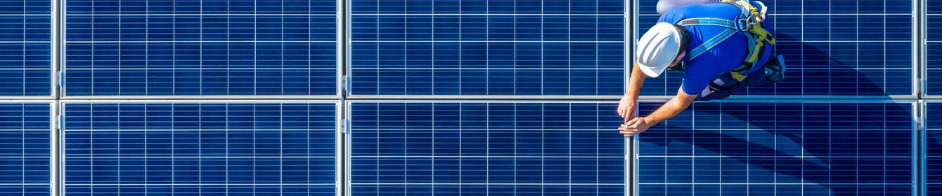
Several layers are added to protect the PV cells so that they can withstand exposure to different weather conditions for over 25 years. Once the solar panel is complete, a junction box is added to the back of the panel which carries the current produced by the panel to either an adjacent module or to the system’s power electronics.
Solution-Processed Solar Cells
Solution-processed solar cells such as perovskite solar cells are readily being explored as a low-cost alternative to silicon solar cells. These cells can be manufactured at low temperatures and without being under vacuum, hence are comparatively cheap to produce.
Solution-processed solar cells need to the thin, so they are usually fabricated using spin-coating or >slot die coating techniques.
Several drawbacks currently prevent solution-based solar cells from becoming the industry standard. Some of the materials used can generate toxic lead during processing steps, and long-term stability of the materials is not yet as good as silicon. Many researchers are focused on finding new materials that can be used to fabricate solution-based solar cells while addressing these issues.
How Are Solar Panels Tested?
Solar panels are tested using controlled conditions to ensure they are working as expected. Sunlight can be replicated using a solar simulator during testing.
Manufacturers put their solar panels into a flash tester once they have been made. The flash tester is set to produce 1000Wm-2 of irradiance, 25°C cell temperature, and an air mass of 1.5 grams. These conditions are known as the standard test conditions (STC) and are used as a reference point for every solar panel's performance.
The testing process measures several electrical parameters that define the solar panel's performance. These include the efficiency, power output, voltage, current, and temperature tolerance. The results are recorded on every panel’s technical specification sheet.
STC are not representative of the conditions that a typical solar panel would experience every day. Therefore, solar panels are also tested using nominal operating cell temperature (NOCT). These conditions are much closer to reality, and include 800 Wm-2 of irradiance, 20°C ambient temperature, and 1ms-1 wind speed. Solar panels are tested using NOCT at a 45° angle, mimicking how they would usually be mounted. Again, the results of this testing are included on the panel’s specification sheet.
Solar Simulator

Learn More
 Monocrystalline vs Polycrystalline Solar Panels
The rise in popularity of solar panels has resulted in several types of solar panels being developed. Each uses slightly different materials or technology to achieve the same goal: convert the sun’s energy into useable electricity. Of these, monocrystalline and polycrystalline solar panels are by far the most popular choices.
Read more... Indoor Photovoltaics: The Future of Indoor Solar Panels
Indoor photovoltaics (IPV) - sometimes known as indoor solar panels - may seem like a contradictory statement, but this technology shows great potential across many industries. IPV consists of conventional photovoltaic technology but instead of using sunlight to promote conductivity, they use energy from artificial light sources. Light-emitting diodes (LEDs), compact fluorescent lamps (CFLs) and halogen lamps are all examples of common artificial lighting that can be used to power indoor solar cells. Therefore, IPVs need to be tested under solar simulators with a modified spectrum to mimic these light sources.
Read more...References
- Sun, L. et al. (2022) 'Recent Progress in Solution-Processed Flexible Organic Photovoltaics', npj Flexible Electronics. doi:10.1038/s41528-022-00222-3.