
Demonstration: Differential Interface

The Challenge of Three-Terminal Device Characterization
Testing two-terminal devices like resistors and diodes typically involves a single coaxial cable connected to a Source-Measure Unit (SMU). However, characterizing three-terminal devices introduces complexities due to precise grounding and signal routing requirements.
Unlike a two-terminal device's simple core-and-shield connection, a three-terminal device's common terminal (e.g., Source of a FET, Emitter of a BJT) must connect to the ground of both SMU channels being used. The other two terminals connect to the respective channel cores. This often results in cumbersome, error-prone setups with standard coaxial cables.
These traditional, often ad-hoc, connection methods sometimes involve multiple coaxial cables, wire stripping, and soldering. They introduce:
- Increased noise susceptibility
- Ground loops
- Impedance mismatches
- Potential device or SMU damage
- Increased sensitivity to electromagnetic interference (EMI)
These issues compromise measurement reliability and reproducibility, especially at higher frequencies or with sensitive devices. This article presents a streamlined solution: the Differential Interface (Coming Soon!).
JFET Characterization with the Differential Interface
We demonstrate the Differential Interface’s ease of use and effectiveness using a J113 N-channel JFET, a readily available and widely used component.
Understanding the JFET
A Junction-Gate Field-Effect Transistor (JFET) is a type of Field Effect Transistor (FET) that uses a reverse-biased p-n junction to control the current flow between the Drain and Source terminals. Unlike MOSFETs, JFETs have a direct connection between the Gate and the channel, formed by the p-n junction.

JFETs are characterized by their high input impedance, low noise, and voltage-controlled current behavior. This makes them well-suited for low-noise amplifiers, analog switches, and impedance-matching. Key parameters that define a JFET’s behavior include the pinch-off voltage (VP), the zero-gate-voltage drain current (IDSS), and the transconductance (gm).
The JFET's three-terminal configuration and sensitivity to proper grounding make it an excellent example to illustrate the benefits of the Differential Interface.
Measurement Setup
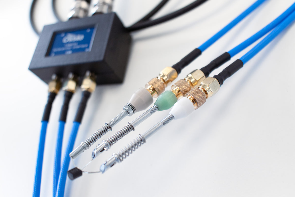
The characterization setup, shown in the Figure 2, consists of the J113 JFET, the Differential Interface, the Ossila Source Measure Unit, and the convenient spring-loaded probe holders from the Ossila Micromanipulators.
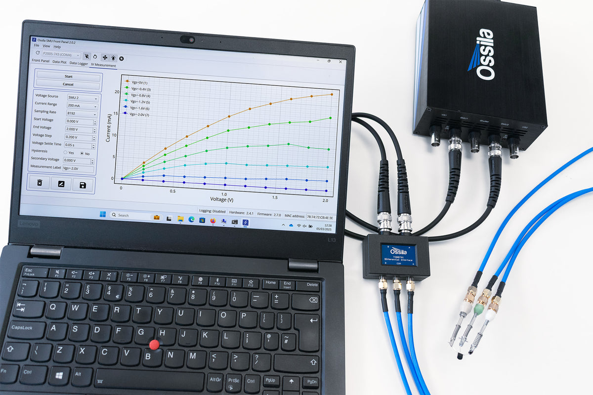
The probes contact the JFET terminals, as illustrated in Figure 3. The Differential Interface is the critical link between the JFET and the SMU.
Differential Interface Configuration
The Differential Interface features three SMA input connectors, each accepting a single-conductor probe for connection to the JFET's Gate, Drain, and Source. Internally (see Figure 4), it routes:
- Source: To the shield (ground) of both SMU input channels, "COM"
- Gate: To the core of SMU1, "A"
- Drain: To the core of SMU2, "B"
- EMI Shielding: The shields of all connected coaxial cables are connected, and grounded via the SMU.

This eliminates manual wiring and external grounding, minimizing noise and ensuring consistent measurements. It removes ambiguity in connecting a three-terminal device to a two-channel SMU.
SMU Configuration
The Ossila Source Measure Unit is configured with two channels:
- SMU1: Sources/measures Gate voltage, VGS, and current, IG.
- SMU2: Sources/measures Drain voltage, VDS, and current, ID.
Using the Differential Interface simplifies setup, reduces setup time, minimizes connection errors, improves accuracy, and could reduce noise from poor solder connections.
JFET Characterization Procedure and Results
The following Python code implements a nested sweep to characterize the J113 JFET. The code controls the Ossila Source Measure Unit to vary both the Drain-Source voltage, VDS, and the Gate-Source voltage, VGS, measuring the resulting Drain current, ID. This generates the JFET's output characteristic curves.
import time
import numpy as np
import xtralien
import matplotlib.pyplot as plt

# --- Configuration Parameters ---
COM_PORT = 10  # USB address of the connected Source Measure Unit (CHANGE THIS IF NEEDED)
CURRENT_RANGE = 1  # Current range to use (refer to SMU manual)
OSR = 6  # Over Sampling Rate (refer to SMU manual)

# --- SMU 1 (Gate) Voltage Sweep Parameters ---
SMU1_V_MIN = -3.0  # SMU 1 minimum voltage (V)
SMU1_V_MAX = 0.0  # SMU 1 maximum voltage (V)
SMU1_V_INC = 0.2  # SMU 1 voltage increment (V)

# --- SMU 2 (Drain) Voltage Sweep Parameters ---
SMU2_V_MIN = 0.0  # SMU 2 minimum voltage (V)
SMU2_V_MAX = 2.0  # SMU 2 maximum voltage (V)
SMU2_V_INC = 0.2  # SMU 2 voltage increment (V)

# --- Data Storage ---
drain_current_data = []  # List to store measured drain current
drain_voltage_data = []  # List to store measured drain voltage
gate_voltage_data = []  # List to store measured gate voltage

# --- SMU Initialization and Control ---
def jfet_characterization(com_port=COM_PORT, current_range=CURRENT_RANGE, osr=OSR):
    """
    Characterizes a JFET using two SMU channels.

    Performs a nested sweep, varying the gate-source voltage (Vgs) for
    different drain-source voltage (Vds) values, and measures the
    resulting drain current (Id).  Plots the output characteristic (Id vs. Vds).

    Args:
        com_port (int): The COM port number of the SMU.
        current_range (int): The current range setting for the SMU.
        osr (int): The oversampling rate setting for the SMU.

    Returns:
        None.  Displays a plot of the JFET output characteristic.
    """

    # Create voltage sweep lists
    smu1_v_list = np.arange(SMU1_V_MAX, SMU1_V_MIN - SMU1_V_INC, -SMU1_V_INC)
    smu2_v_list = np.arange(SMU2_V_MIN, SMU2_V_MAX + SMU2_V_INC, SMU2_V_INC)

    with xtralien.Device(f'COM{com_port}') as smu:
        # Initialize and enable SMU channels
        for smu_channel in ['smu1', 'smu2']:
            smu[smu_channel].set.range(current_range)
            time.sleep(0.05)
            smu[smu_channel].set.osr(osr)
            time.sleep(0.05)
            smu[smu_channel].set.enabled(True)
            time.sleep(0.05)

        # Nested sweep:  Outer loop is Vds, inner loop is Vgs
        for smu2_v_set in smu2_v_list:
            smu['smu2'].set.voltage(smu2_v_set)
            time.sleep(0.1)

            for smu1_v_set in smu1_v_list:
                smu['smu1'].set.voltage(smu1_v_set)
                time.sleep(0.1)

                # Measure both SMU channels
                smu1_v, smu1_i = smu['smu1'].measure()[0]
                smu2_v, smu2_i = smu['smu2'].measure()[0]

                # Store measured data
                drain_voltage_data.append(smu2_v)
                gate_voltage_data.append(smu1_v)
                drain_current_data.append(smu2_i)


    # Disable SMU channels and set output to 0 V
    for smu_channel in ['smu1', 'smu2']:
        smu[smu_channel].set.voltage(0)
        time.sleep(0.05)
        smu[smu_channel].set.enabled(False)
        time.sleep(0.05)

    # --- Data Processing and Plotting ---
    # Convert lists to NumPy arrays and scale current to mA
    drain_current_array = np.array(drain_current_data) * 1000
    drain_voltage_array = np.array(drain_voltage_data)
    gate_voltage_array = np.array(gate_voltage_data)

    # Create the output characteristic plot (Id vs. Vds for different Vgs)
    rounded_gate_voltage = np.round(gate_voltage_array, 2)
    unique_gate_voltages = np.unique(rounded_gate_voltage)

    plt.figure()  # Create a new figure
    for vg_val in unique_gate_voltages:
        indices = np.where(rounded_gate_voltage == vg_val)[0]
        id_subset = drain_current_array[indices]
        vd_subset = drain_voltage_array[indices]
        label_string = f"V$_{{GS}}$ = {vg_val:.2f} V"  # Use f-string for formatting
        plt.plot(vd_subset, id_subset, label=label_string)

    plt.xlabel("V$_{DS}$, Drain-Source Voltage (V)")
    plt.ylabel("I$_D$, Drain Current (mA)")
    plt.title("JFET Output Characteristic")  # Add a title
    handles, labels = plt.gca().get_legend_handles_labels()
    plt.legend(handles[::-1], labels[::-1], loc="best")  # Reverse ordering of legend entries so 0V is at the top
    plt.grid(True)
    plt.show()

if __name__ == '__main__':
    jfet_characterization()
The Gate-Source cut-off voltage of the JFET is around VGS = -2.0 V, which is consistent with the datasheet specifications.

Conclusion
The Differential Interface simplifies JFET characterization, offering ease of use, accuracy, and versatility. The streamlined setup and provided Python code significantly reduced measurement time and effort. While focused on a JFET, the principles apply to other three-terminal devices (BJTs, MOSFETs, etc.). Future work could explore automated parameter extraction (VP, IDSS, and gm from the transfer characteristic curve) and temperature-dependent characterization.
Contributors
Written by
Product Developer
Diagrams by
Graphic Designer