How does phosphorene compare to graphene and other 2D materials?
Single-layer black phosphorus’ hole mobility compares favourably with Transition Metal Dichalcogenide Monolayers (TMDCs) but is orders of magnitude below that of graphene. Thermal conductivity is again below that of graphene, but competitive with TMDCs. Transistors fabricated from few-layer phosphorene display a high on/off ratio of 105 — significantly better than unmodified graphene, but falling behind TMDCs.
Phosphorene can be seen as an intermediary material, taking favourable properties of graphene and TDMCs but dispensing with their undesirable characteristics.
A comparison between some of the relevant optoelectronic properties of 2D materials is given in the table below.
| Graphene | 2D TMDC | Phosphorene | |
|---|---|---|---|
| Band Gap | 0 |
2 eV (WS2) 1.9 eV (MoS3) |
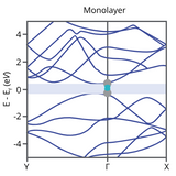
0.3 eV (bulk) – 1.88 eV (monolayer) |
| Carrier Mobility | 2 x 105 cm2V-1s-1 |
~1000 cm2V-1s-1 (WS2)[3] ~350 cm2V-1s-1 (MoS2)[3] |
~1000 cm2V-1s-1 (WS2) [6] |
| Thermal Conductivity | 5000 Wm-1K-1 |
32 Wm-1K-1 (WS2) [4] 35 Wm-1K-1 (MoS2) [5] |
86 (34) Wm-1K-1 in ZZ (AC) direction (few-layer) [7] |
| On/Off Ratio | ~100 [9] |
~107 (WS2) [10] ~108 (MoS2) [11] |
105 [8] |
Black Phosphorus

Learn More
 Black Phosphorus Properties
The optical, electronic, and mechanical properties of phosphorene differ from that of the bulk state due to combinations of factors.
Read more... Black Phosphorus Uses and Applications
Due to the unique properties, exfoliated monolayer and few-layer black phosphorus have potential for a wide range of applications in electronics and optoelectronics.
Read more...