I301 Triple Cation Perovskite Solar Cells Processing

Below is a condensed summary of our fabrication routine for standard architecture devices using our I301 Triple Cation Perovskite Precursor Ink. This recipe is based on the one described by Saliba et al (2018).
We recommend pre-weighing all solutions, dopants, and precursors with a calibrated microbalance before starting the fabrication process.
Standard Architecture Device Fabrication
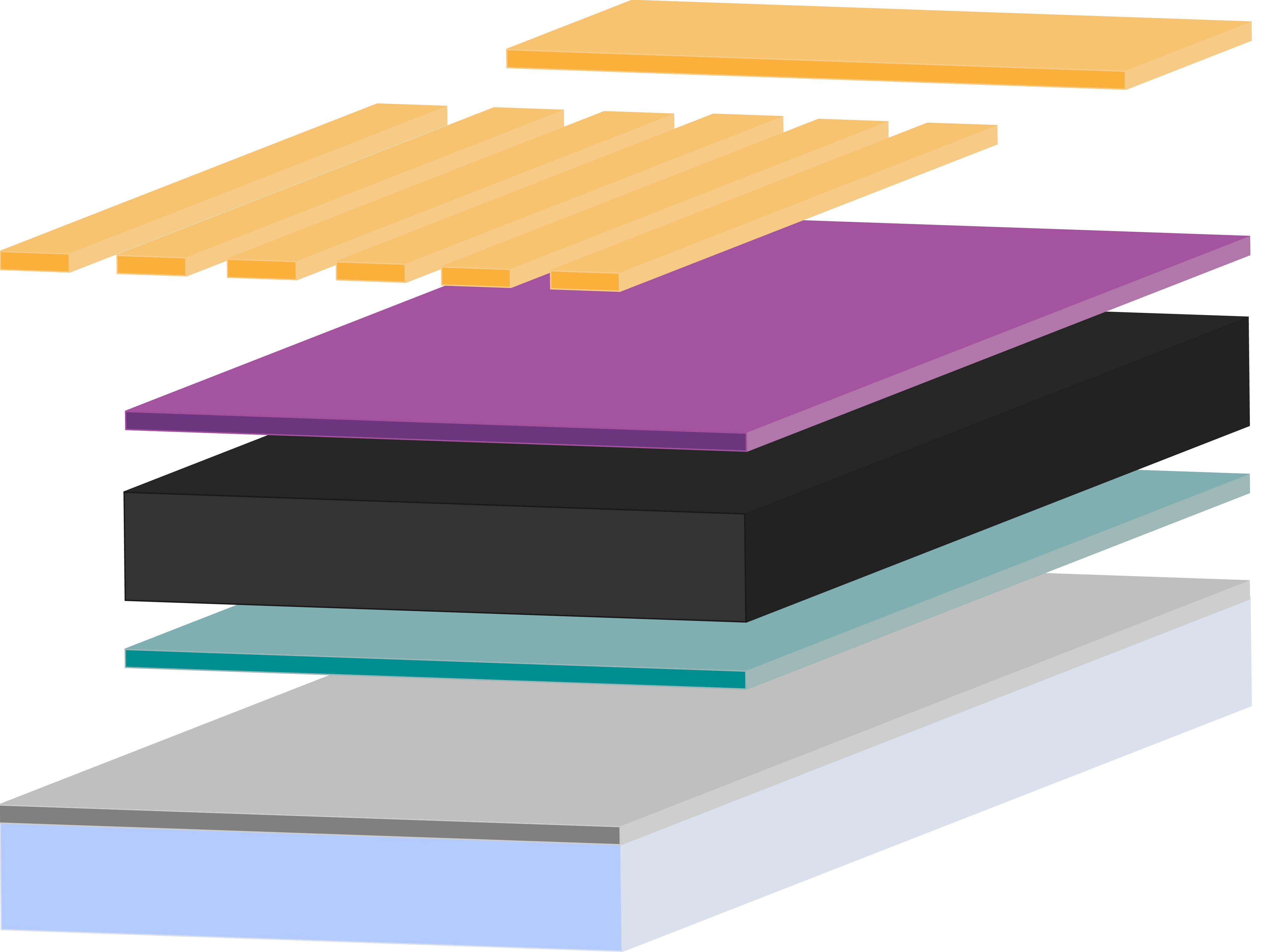
ITO-coated glass/SnO2/perovskite/Spiro-OMeTAD/Au
-
ITO etching:
- A complete guide to FTO/ITO etching can be found on our FTO product page along with an instructional video
-
Substrate cleaning:
- Rub ITO between (gloved) fingers with DI water containing Hellmanex then rinse with water. This is a very important step in the cleaning process.
- Rinse thoroughly in boiling DI water, sonicate for a few minutes in DI water if you want to be extra cautious.
- Rinse and sonicate ITO for 15 minutes in isopropyl alcohol (IPA)
- Dry ITO using filtered compressed gas
- Place the ITO into the UV ozone cleaner and clean for 15-20 minutes
-
SnO2 ETL deposition:
- Create a 4:1 suspension of 15% SnO2 nanoparticles in DI water
- Statically spin coat 50ul of SnO2 onto substrate fresh from UV ozone 3000rpm for 30s.
- Using a cotton bud and DI water, wipe away the SnO2 layer where the conductive busbars are to be deposited.
- Anneal for 40 mins at 150°C.

-
Perovskite deposition (in glove box):
- Transfer the substrates into an inert environment glove box.
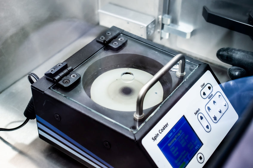
- Place substrates inside the spin coater.
- Dispense 35 μl of I301 ink onto the substrate. Spin the substrate at 1000 rpm for 10s. After this initial spin step, increase the speed to 3000 rpm over 28s. 13 seconds into the 3000 rpm spin step, dispense 100μl of ethyl acetate to quench the perovskite and leave to spin for a further 15 s (the quenching should be done using a continuous stream of solvent over ~1 s)
- Place substrate back onto the hotplate at 130°C for 10 minutes.
-
Spiro-OMeTAD deposition (in glove box):
- Prepare the following solutions:
- Spiro-OMeTAD at a concentration of 85 mg/ml in chlorobenzene
- Li-TFSI at a concentration of 500 mg/ml in acetonitrile
- TBP at a volumetric percentage of 98%
- FK209 Co (III) TFSI at a concentration of 300 mg/ml in acetonitrile
- Combine 1000 μl Spiro-OMeTAD, 20μl Li-TFSI, 34μl TBP and 11μl of FK209 Co (III) TFSI
- Ensure complete solvation of dopants within solution (e.g. vortex for 5 minute/stir overnight) and filter mixture directly before use.
- Start spinning at 4000 rpm for 30 seconds
- Dynamically dispense 25 µl of the combined solution onto the perovskite to create a thin even layer.
-
Spiro-OMeTAD oxidation and anode deposition:
- Remove devices from the glove box. The spiro-OMeTAD layer will require further oxidation to achieve optimal device performance; this should be achieved after 12 hours of storage in air
- Using tweezers or a razor, scratch away the perovskite and spiro-OMeTAD layer where the conductive busbars are to be deposited
- Using thermal evaporation, deposit an 80 nm layer of gold through a shadow mask to define an active area for your device (we recommend the use of Ossila's multi electrode/busbar mask for optimal device performance)
- Devices measured immediately after being taken out of the glove box have a PCE 1% lower on average than devices left in air for 12 hours and can be up to 3% lower in extreme cases.
Perovskite Materials

Learn More
Silicon is the most commonly used material in photovoltaic (PV) technology. In recent times perovskite materials have generated much excitement in the field of solar cell research. Here we discuss the pros and cons of each in addition to their use in conjunction with one another.
Read more... Perovskite Solar Cell Layers
Perovskite solar cells need several layers in order to absorb light, then separate and extract charge. In basic terms, a planar PSC needs an absorbing perovskite layer sandwiched in between a hole transport layer and an electron transport layer.
Read more...References
- How To Make Over 20% Efficient Perovskite Solar Cells In Regular (N-I-P) And Inverted (P-I-N) Architectures. M. Saliba et al. Chem. Mater. 30 (2018) 4193–4201 DOI: 10.1021/acs.chemmater.8b00136.