Hexagonal Boron Nitride (h-BN) Film
CAS Number 10043-11-5
2D Materials, Hexagonal Boron Nitride, Low Dimensional Materials, MaterialsLow price, high purity 2D hexagonal boron nitride (h-BN) film
Suitable for the creation of single or few-layer sheets via mechanical or liquid exfoliation
Technical Data | MSDS | Literature and Reviews
Hexagonal boron nitride (h-BN) (CAS number 10043-11-5) has a honeycomb structure based on sp2 covalent bonds similar to graphene. Due to the similarity it is also known as “white graphene”. Unlike graphene, h-BN exhibits a wide band gap. This band gap uniquely transitions from indirect in its bulk form to direct when reduced to a monolayer.
High Purity
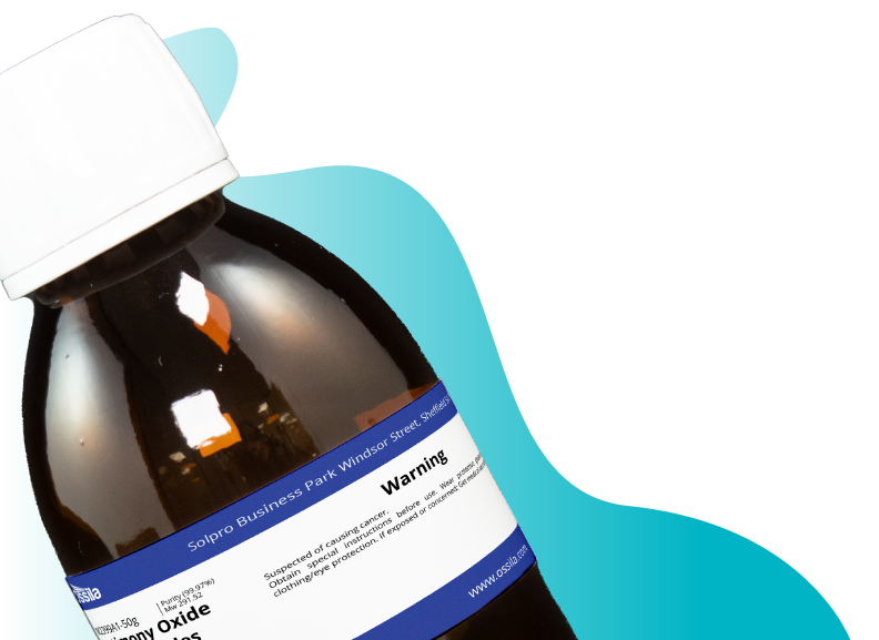
High purity ≥99.99% Hexagonal Boron Nitride Crystal
Worldwide shipping
Quick and reliable shipping
Low price
Low price Hexagonal Boron Nitride (h-BN)
Ultrathin Films
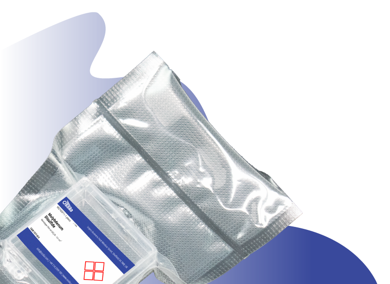
Available in monolayer and few-layer films
h-BN is considered an insulator, and is used as a sub-layer material for any other 2D material in electronic devices. However, it has exotic opto-electronic properties (e.g. wide bandgap and low dielectric constant) along with mechanical robustness, high thermal conductivity and chemical inertness. h-BN is widely used as a dielectric substrate in electronic and optical devices for graphene and other 2D-layered semiconductors (e.g. transition metal dichalcogenides TMDs).
2D h-BN has no absorption in the visible range, but has absorption in the ultraviolet region with good photoluminescence.
Hexagonal boron nitride (h-BN) few-layer film, often referred to as h-BN nanosheets (h-BNNs), has an ultra-flat surface without dangling bonds. Due to its oxidation resistance even at high temperatures (up to 1000 oC) and chemical resistance to both acids and bases, it is believed to be a better substrate than silicon.
*Custom made size and substrates are also available
- Glass (1 cm × 1 cm, 1 cm × 2 cm, 2 cm × 2 cm or custom-made sizes)
- Sapphire (1 cm × 2 cm, 2 cm × 2 cm or custom-made sizes)
- Silicon (1 cm × 2 cm, 2 cm × 2 cm or custom-made sizes)
- Quartz (1 cm × 2 cm, 2 cm × 2 cm or custom-made sizes)
Technical Data
| CAS Number | 10043-11-5 |
| Full Name | Hexagonal boron nitride |
| Chemical Formula | BN |
| Molecular Weight | 24.82 g/mol |
| Preparation | Synthetic - Chemical Vapour Transport (CVT) |
| Structure | Hexagonal (2H) |
| Electronic Properties | 2D Materials - insulator/semiconductor |
| Melting Point | 2,973 °C (sublimates) |
| Colour | Colourless |
| Synonyms | White graphene, hexagonal BN, h-BN, hBN |
| Classification / Family | 2D materials, Organic electronics, Materials science |
| Purity | ≥99% |
Monolayer Film
| Substrate | SiO2/Si | PET | Sapphire | Quartz |
| Product Code | M2161F11 | M2162F11 | M2319F11 | M2320F11 |
| Size | 1 cm × 1 cm* | 1 cm × 1 cm* | 1 cm × 1 cm* | 1 cm × 1 cm* |
| Growth Method | CVD synthesis | CVD synthesis | CVD synthesis | CVD synthesis |
| Appearance | Transparent | Transparent | Transparent | Transparent |
| Purity | >99% | >99% | >99% | >99% |
| Transparency | >97% | >97% | >97% | >97% |
| Coverage | >95% | >95% | >95% | >95% |
| Number of Layers | 1 | 1 | 1 | 1 |
| Sheet Resistance | n.a. | n.a. | n.a. | n.a. |
| Transfer method | Wet chemical transfer | Wet chemical transfer | Wet chemical transfer | Wet chemical transfer |
| Substrate Thickness | 300 nm (oxide layer) | 250 µm | 300 µm | 1 mm |
| Bandgap | Direct ~ 6 eV | Direct ~ 6 eV | Direct ~ 6 eV | Direct ~ 6 eV |
Few-Layer Film
| Substrate | SiO2/Si | PET | Sapphire | Quartz |
| Product Code | M2163F11 | M2164F11 | M2321F11 | M2322F11 |
| Size | 1 cm × 1 cm* | 1 cm × 1 cm* | 1 cm × 1 cm* | 1 cm × 1 cm* |
| Growth Method | CVD synthesis | CVD synthesis | CVD synthesis | CVD synthesis |
| Appearance | Transparent | Transparent | Transparent | Transparent |
| Purity | >99% | >99% | >99% | >99% |
| Transparency | >97% | >97% | >97% | >97% |
| Coverage | >95% | >95% | >95% | >95% |
| Number of Layers | 2 - 6 | 2 - 6 | 2 - 6 | 2 - 6 |
| Bandgap | Indirect 5.955 eV | Indirect 5.955 eV | Indirect 5.955 eV | Indirect 5.955 eV |
| Sheet Resistance | n.a. | n.a. | n.a. | n.a. |
| Transfer method | Wet chemical transfer | Wet chemical transfer | Wet chemical transfer | Wet chemical transfer |
| Substrate Thickness | 300 nm (oxide layer) | 250 µm | 300 µm | 1 mm |
Pricing Table
| Product Code | Form | Package/Substrates* | Price |
| M2161F11 | Monolayer Films | SiO2/Si - 1 Each | £200 |
| M2161F11 | Monolayer Films | SiO2/Si - 2 Each | £340 |
| M2162F11 | Monolayer Films | PET - 1 Each | £200 |
| M2162F11 | Monolayer Films | PET - 2 Each | £340 |
| M2319F11 | Monolayer Films | Sapphire - 1 Each | £200 |
| M2319F11 | Monolayer Films | Sapphire - 2 Each | £340 |
| M2320F11 | Monolayer Films | Quartz - 1 Each | £200 |
| M2320F11 | Monolayer Films | Quartz - 2 Each | £340 |
| M2163F11 | Few-Layer Films | SiO2/Si - 1 Each | £200 |
| M2163F11 | Few-Layer Films | SiO2/Si - 2 Each | £340 |
| M2164F11 | Few-Layer Films | PET - 1 Each | £200 |
| M2164F11 | Few-Layer Films | PET - 2 Each | £340 |
| M2321F11 | Few-Layer Films | Sapphire - 1 Each | £200 |
| M2321F11 | Few-Layer Films | Sapphire - 2 Each | £340 |
| M2322F11 | Few-Layer Films | Quartz - 1 Each | £200 |
| M2322F11 | Few-Layer Films | Quartz - 2 Each | £340 |
*typical representative size, areas/dimensions may vary
**item with a lead time of 4 - 6 weeks, please contact for more information
Shipping is free for qualifying orders.
MSDS Documents
Monolayer Film
 Hexagonal boron nitride monolayer film SiO2/Si
 Hexagonal boron nitride monolayer film PET
 Hexagonal boron nitride monolayer film sapphire
 Hexagonal boron nitride monolayer film quartz
Few-Layer Film
 Hexagonal boron nitride few-layer film SiO2/Si
 Hexagonal boron nitride few-layer film PET
 Hexagonal boron nitride few-layer film sapphire
 Hexagonal boron nitride few-layer film quartz
Literature and Reviews
- Hexagonal boron nitride is an indirect bandgap semiconductor, G. Cassabois et al., Nat. Photon., 10, 262–266 (2016);DOI: 10.1038/NPHOTON.2015.277.
- Graphene, hexagonal boron nitride, and their heterostructures: properties and applications, J. Wang et al., RSC Adv., 7, 16801 (2017); DOI: 10.1039/c7ra00260b.
- Two dimensional hexagonal boron nitride (2D-h-BN): synthesis, properties and applications, K. Zhang et al., J. Mater. Chem. C, 5, 11992 (2017); DOI: 10.1039/c7tc04300g.
Related Products
We stock a wide range of 2D materials available to purchase online. Please contact us if you cannot find what you are looking for.


