
ITO Glass Substrates, 20 x 15 mm, OFET and Sensing
Materials, Substrates and Fabrication
Pre-Patterned ITO Substrates for OFET and Sensing
For simple fabrication and testing
Transmittance | Characterization | Related Products | Resources and Support
Pre-patterned ITO substrates designed for the fabrication and characterization of transistors and sensing devices without the need for vacuum evaporations or probe stations. Devices can be produced and tested with significantly increased simplicity, making the system ideal for reducing costs of material screening experiments.
Specifications
| Substrate Size | 20 mm x 15 mm |
|---|---|
| Pack Size | 100 substrates per standard pack |
| Thickness | 1.1 mm |
| Channel Dimensions* (W x L) |
S161: 30 mm × 50 μm S162: 30 mm × 50 μm, 75 μm, 100 μm, 150 μm, and 200 μm |
| Glass Type | Polished soda lime, float glass |
| Substrate Coating | Fully oxidized ITO |
| ITO Thickness | 100 nm |
| ITO Resistance | 20 Ω/square |
| Glass Roughness | <1 nm RMS (by AFM) |
| ITO Roughness | 1.8 nm RMS (by AFM) |
* There may be a batch-to-batch variation of ±10 μm in the channel length.


Transmittance of ITO Substrates

Characterization

Characterization courtesy of Richard T Grant.
Related Products


Resources and Support
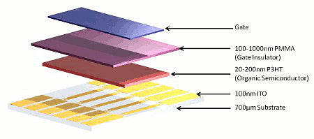
Evaporation-Free OFET Substrates
The substrates contain pre-patterned ITO source-drain contacts onto which the semiconductor is deposited before a gate insulator is spun on top and finally the gate material finishes the device. All of these layers can be deposited from solution, including the gate using a synthetic metal (such as PEDOT:PSS), meaning no evaporation shadow masks are required. It is possible to make fully-functioning OFETs by solution processing alone, eliminating vacuum evaporation processes.
The substrates are also designed to work with a wide variety of different material systems and deposition techniques. As such, vacuum-deposited semiconductors, gate insulators, and gates can also be used with the appropriate shadow mask.
The pre-patterned OFET substrates consist of interdigitated ITO fingers to act as the source-drain electrodes. The relatively large channel sizes work to minimize contact effects, so it is less important to match the energy levels of the organic semiconductor and contacts. As such, the intrinsic Poole Frenkel limited mobility of a material can be more easily assessed independent of the HOMO level. The 30 mm channel width also has the additional benefit of producing larger currents, making testing and measurement quicker and requiring less sensitive (and less expensive) equipment.
The transparent nature of the ITO/glass also means that opto-electric experiments can be done with ease (photoconductivity, photo-induced doping in the presence of oxygen, sensing).