Evaporation Stack for OFETs, High Density
Substrates and FabricationHigh Density Evaporation Stack for OFETs
Enabling accurate deposition resolution
Overview | Specifications | Resources
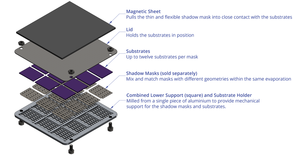
The evaporation stack holds the source-drain shadow masks (sold separately) and substrates in close contact for thermal evaporation. This is crucial for device fabrication because the source-drain channel is the most critical feature on an OFET. For use with the Ossila high-density OFET source-drain evaporation masks and Silicon Oxide Substrates.
Specifications
The key component is the lower support, which is milled from a solid block of aluminum to provide high-precision recesses for individual shadow masks and substrates, and allows mixing-and-matching of shadow masks within a single evaporation.
| Size | 75 mm x 75 mm |
| Thickness | 2 mm (exc. bolts) |
| Material | Lower support: milled aluminum Lid: stainless steel Magnetic sheet: vinyl-laminated polymer resin with ferrite powder |
| Substrate capacity | Square design: 12 substrates |

System Overview
Schematic diagrams showing how the high-density FET evaporation masks work together for:
For interdigitated FETs, the source-drain, active area, and gate masks need to be replaced with the corresponding versions.


