TIPS Pentacene, p-type organic semiconductor with a high purity of >99.9%
High hole mobility and excellent air stability, 6,13-Bis(triisopropylsilylethynyl)pentacene, 373596-08-8
TIPS-Pentacene is tri-isopropylsilyly-ethynyl (TIPS) substituted pentacene at 6- and 13-positions of the conjugated core. The substituted TIPS functional groups extend the conjugation further to the branches to provide further stability, enhance solubility for solution processing for low-cost and large-area fabrication of organic thin-film transistors (OTFTs).
TIPS pentacene has been developed as a p-type organic semiconductor, and demonstrates high hole mobility and excellent air stability with great solution processability. The substitution of two bulky side groups can not only significantly enhance the solubility of TIPS-pentacene in most of the common solvents but also prevent the middle acene from oxidation and degradation. The tri-isopropylsilyly-ethynyl side groups can also interrupt the edge-to-face interaction of the aromatic ring to avoid the herringbone packing motif in neat pentacene. The ethynyl groups keeps the bulky side tri-isopropylsilyly groups away from the aromatic ring to allow π-π stacking between adjacent TIPS pentacene molecules.
In general, polymer/TIPS pentacene blends have been used to improve film morphology and reduce crystal misorientation since TIPS-pentacene crystalline films are highly anisotropic, which could lead to significant variations in device performance.
A high-purity TIPS-Pentacene for use in organic field-effect transistors (OFETs). TIPS-Pentacene is widely used as a high performance small molecule for OFET applications, with a mobility in excess of 1 cm2/Vs having being achieved in the literature. It has excellent solubility in a range of common organic solvents, and a good ambient stability - making it easy to process into devices. Ossila's TIPS-pentacene has been produced with a purity of >99.9%.
TIPS-Pentacene from Ossila was used in the high-impact paper (IF 18.81), Self-Assembled, Millimeter-Sized TIPS-Pentacene Spherulites Grown on Partially Crosslinked Polymer Gate Dielectric, H. Yoo et al., Adv. Funct. Mater., 3658-3665 (2015); DOI: 10.1002/adfm.201501381.
Please note that TIPS-Pentacene is unavailable to buyers in the USA. Any incoming orders from the USA for TIPS-Pentacene will not be processed.
General Information
| Full name | 6,13-Bis(triisopropylsilylethynyl)pentacene |
|---|---|
| Synonyms | TIPS-pentacene |
| CAS number | 373596-08-8 |
| Chemical formula | C44H54Si2 |
| Molecular weight | 639.07 g/mol |
| Solvents | Anisole, butylbenzene, chlorobenzene, chloroform, dichlorobenzene, tetrahydrofuran, toluene, xylene |
| Classification / Family | Molecular semiconductors, Small molecule semiconductor, Organic Field-Effect Transistors (OFETs), soluble semiconductor materials, Pentacene derivatives |
Product Details
| Purity | > 99 % (HPLC) > 99% (1H-NMR) |
|---|---|
| Melting point | 259 °C (DSC) |
| Appearance | Dark blue solid |
Chemical Structure
Characterisation
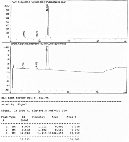
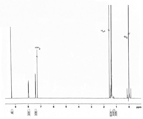
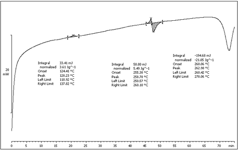
OFET fabrication procedure
Abstract
We have achieved a mobility of approximately 0.92 cm2/Vs using TIPS-Pentacene for top contact OFETs with a drop casting protocol. The TIPS-Pentacene film is obtained through slow crystallisation growth at high temperature (50°C), in solvent saturated ambient, over silicon oxide substrates treated with phenyl-terminated silane molecules.
Results
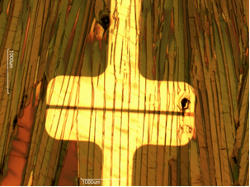
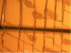
The image below depicts the best performance OFET, showing how the boundaries of the crystals forming the crystallite domain have boundaries parallel to the channel length. Cracks perpendicular to the growth direction are also clearly visible. These cracks act as defects (bottlenecks for charge transport) and must be minimised in order to obtain high-performing OFETs.
FET measurements
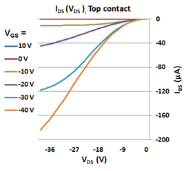
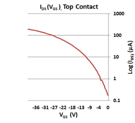
The table below summarises the mobility and threshold voltage for the three PTES-treated substrates, taking an average of 75% of the 15 OFET devices to minimise the maximum and minimum outliers.
| Devices Measured | Mobility (cm2/Vs) | VT (V) |
|---|---|---|
| 15 | 0.28 +/- 0.06 | -5.14 +/- 2.75 |
Drop casting details
The direction of the crystal growth, and therefore the orientation of the crystal axes (with respect to the channel length), can be controlled by imposing a preferential drying direction to the drop casted solution. This is achieved by positioning the substrate inside a Petri dish at a 3.5° angle with respect to the horizontal line of a perfectly flat hot plate. Substrates are placed inside the Petri dish in a manner such that the length of the channel is perpendicular to the receding direction of the drying solution. Drop casting is carried out using a pipette with the substrate at a temperature of 50°C. The lid was put back immediately afterwards to trap the solvent vapour and create a vapour-saturated condition inside the Petri dish.
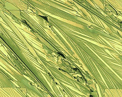
Images below taken of thin films of TIPS-pentacene deposited by spin casting and drop casting from toluene (10 mg/ml) on SiO2, showing the strong crystallisation behaviour in slow dried films.

|

|
|
Experimental
OFET device specifications
This table shows details of the substrates used in this fabrication routine.
| Substrates | Ossila silicon/silicon dioxide substrates (S146) |
|---|---|
| Substrate size | 20 x 15 mm |
| Gate conductivity | 1-30 Ω·cm (Boron doped) |
| Silicon oxide thickness | 300 nm |
| Device per substrates | Five, common gate |
| Channel length | 30 µm |
| Channel width | 1000 µm |
| OFET architecture | Top contact, bottom gate |
| Source-Drain patterning | Thermal evaporation using Source-Drain Deposition Mask for Low Density OFETs |
TIPS-Pentacene Solution Preparation
Preparation of the stock solution took place in a glove box (O2 << 10 ppm; H2O). The solution used for drop casting was prepared only when needed. TIPS-pentacene is relatively resilient to oxidation at room temperature. However, long permanence in normal ambient condition (>24 hrs) can result in molecular degradation and increased water content of the solution.
- TIPS-pentacene dissolved in anhydrous toluene, 10 mg/ml, to make stock solution
- The stock solution is placed on a hotplate at 60°C for 1 hour at 1000 rpm with a magnetic stirrer
- Solution was then filtered with 0.45 µm filter into a new vial
- Required amount was diluted with anhydrous toluene to 2 mg/ml
Substrate cleaning
- 1% Hellmanex III solution in hot DI water
- Sonicate for 5 min in hot water
- Rinse twice in hot water
- IPA, Sonicate 5 min in hot water
- Rinse twice in DI water (cold)
- Store substrates in DI water
- UV Ozone treatment for 5 min
Surface Treatments
- PTES (Trichloro(phenethyl)silane) treatment: 3 mMol in toluene for 15 hrs in glove box at 90°C or, alternatively
- PTS (Trichloro(phenyl)silane) treatment: 3% in weight in toluene at 90°C for 15 hrs in glove box
- Substrates rinsed twice in glove box with toluene, then blow dried and brought outside a glove box
- Sonicated in toluene for 10 minutes and blow dried
- Rinsed with 2 ml of acetone and blow dried
- Rinsed with 2 ml of IPA and blow dried
- Put in glove box on hotplate at 150°C for 5 min
TIPS-pentacene drop casting
- Pipetted 50 μl of TIPS solution (2 mg/ml) onto each substrate, which were sitting within a petri dish
- Covered with glass lid for 5 minutes on a hot plate at 50°C
- Hot plate switched off and left to cool down to close to room temperature
- Using cleanroom swabs wetted with toluene, wiped the substrates clean with the exception of the area over which the drain and source were to be deposited
- Loaded the substrates into the evaporation stack for low density OFETs
Deposition of top contact gold
- Loaded Edwards Auto 306 thermal evaporator
- Evaporator left to pump down to low pressure (ca. 2 x 10⁻⁶ mBar)
- Deposited 80 nm of gold on TIPS-pentacene-coated substrates
OFETs were measured using an Ossila Test Board for Low-Density OFETs (E222) under air.

